 ChipApex | Global Electronic Components Supplier
SEARCH
Search Product
Search Post
— IC芯片 | 连接器 | 传感器 | 被动器件 —
Search productSearch post
— IC芯片 | 连接器 | 传感器 | 被动器件 —
Consult the customer manager about the wholesale price.
consultation hotline:86-132-6715-2157
email:[email protected]
Contact the product manager for consultation. One-stop consultation is available.
Do you want a lower wholesale price? Please send us your inquiry and we will reply immediately.
The PBSS3515VS,115 is a PNP low VCEsat double transistor housed in an SOT666 ultra-small and flat lead Surface-Mounted Device plastic package. It features a total power dissipation of 300 mW and a collector-emitter voltage (VCEO) of -15 V per transistor. The device supports a maximum collector current (IC) of -500 mA and offers a DC current gain (hFE) ranging from 90 to 200 depending on operating conditions. Transition frequency (fT) reaches up to 280 MHz at -100 mA. The package dimensions are 1.6 mm x 1.2 mm x 0.55 mm, providing self-alignment during soldering due to straight leads.
Verify the component marking code '35' against the datasheet to confirm authenticity. Ensure the ordering suffix ',115' matches the specific reel or tape configuration required for automated assembly processes. Confirm that the application environment remains within the specified non-automotive qualification limits provided by Nexperia.
Select this component when space constraints require replacing two discrete transistors with a single dual unit. Consider the -15 V collector-emitter voltage rating and -500 mA current capability for circuit design. Evaluate the thermal resistance characteristics if operation exceeds standard ambient temperature ranges without adequate PCB copper heat sinking.
This part belongs to the PBSS series of low VCEsat double transistors manufactured by Nexperia. It serves as the PNP complement to the NPN PBSS2515VS model. Both devices utilize the same SOT666 package footprint, allowing designers to implement complementary push-pull configurations within minimal board space while maintaining consistent thermal profiles.
Direct replacement options include other PNP double transistors in the SOT666 package with matching -15 V ratings. Verify pinout compatibility between TR1 and TR2 emitters and collectors before substitution. Ensure the alternative device meets the same 300 mW total power dissipation requirement under similar thermal conditions.
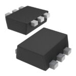 PBSS3515VS,115
The activity of extra discounts on wholesale prices is in full swing…
Please fill in your contact information and we will send you the latest wholesale price list.





