 ChipApex | Global Electronic Components Supplier
SEARCH
Search Product
Search Post
— IC芯片 | 连接器 | 传感器 | 被动器件 —
Search productSearch post
— IC芯片 | 连接器 | 传感器 | 被动器件 —
Consult the customer manager about the wholesale price.
consultation hotline:86-132-6715-2157
email:[email protected]
Contact the product manager for consultation. One-stop consultation is available.
Do you want a lower wholesale price? Please send us your inquiry and we will reply immediately.
The PBSS4021SP,115 is a PNP/PNP Breakthrough In Small Signal (BISS) transistor manufactured by Nexperia. It is housed in an SOT96-1 (SO8) surface-mount package with eight leads and a body width of 3.9 mm. The device features a collector-emitter voltage (VCEO) of -20 V and a continuous collector current (IC) of -6.3 A. Peak collector current (ICM) reaches -15 A for single pulses up to 1 ms. Total power dissipation is rated at 0.73 W on FR4 PCBs and 1.7 W on ceramic substrates. The transition frequency is 105 MHz, and the maximum junction temperature is 150 °C.
Verify the component against the official Nexperia datasheet specifications before integration. Confirm that the ordering suffix matches the required packing method, as variations exist between tape and reel quantities. Ensure thermal design accounts for the specific PCB material and copper weight used in the final assembly to maintain safe operating temperatures.
Select this component when low saturation voltage and high current density are critical within an SO8 footprint. Evaluate thermal resistance based on the target substrate, as dissipation varies significantly between standard FR4 and ceramic boards. Verify that the required peak current does not exceed the 15 A limit during transient conditions.
This part belongs to the BISS transistor family designed for compact power applications. It serves as the PNP/PNP complement to the NPN/NPN PBSS4021SN variant. Both share similar electrical characteristics but differ in polarity and package pinout configuration for dual-channel operation.
The PBSS4021SN is the NPN/NPN complementary counterpart within the same product family. Direct substitution requires verifying polarity compatibility and ensuring the circuit design supports the opposite charge carrier type.
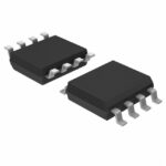 PBSS4021SP,115
The activity of extra discounts on wholesale prices is in full swing…
Please fill in your contact information and we will send you the latest wholesale price list.




