 ChipApex | Global Electronic Components Supplier
SEARCH
Search Product
Search Post
— IC芯片 | 连接器 | 传感器 | 被动器件 —
Search productSearch post
— IC芯片 | 连接器 | 传感器 | 被动器件 —
Consult the customer manager about the wholesale price.
consultation hotline:86-132-6715-2157
email:[email protected]
Contact the product manager for consultation. One-stop consultation is available.
Do you want a lower wholesale price? Please send us your inquiry and we will reply immediately.
The PBSS4021SPN is a Breakthrough In Small Signal (BISS) transistor containing an NPN and PNP pair in a SOT96-1 (SO8) package. It features a collector-emitter voltage of 20 V, with continuous collector currents of 7.5 A for the NPN and -6.3 A for the PNP. Peak collector current reaches 15 A. The device exhibits low saturation resistance, typically 35 mΩ for the NPN at 5 A, and 54 mΩ for the PNP at -5 A. DC current gain ranges from 100 to 550 depending on current levels. Total power dissipation varies from 0.73 W to 1.7 W based on PCB mounting conditions.
Verify the specific ordering suffix against the manufacturer's official documentation to confirm packing methods and tape-and-reel specifications. Ensure the component matches the exact SOT96-1 package dimensions and pinout configuration required by the design footprint. Cross-reference the marking code '4021SPN' to authenticate the device origin and revision status before integration into production.
Select this component when space constraints require a compact dual-transistor solution with high current handling capabilities. Evaluate thermal performance requirements against the specified junction-to-ambient resistance values for the intended PCB copper area. Confirm that the 20 V rating provides sufficient margin for the maximum operating voltage and transient spikes present in the target application circuit.
This part belongs to Nexperia's BISS transistor family, designed to replace multiple discrete components. It integrates complementary NPN and PNP structures into a single surface-mount package. This integration simplifies board layout and improves switching consistency between paired transistors compared to using separate individual devices.
The datasheet lists the PBSS4021SN and PBSS4021SP as complementary variants within the same product line. Verify pin compatibility and electrical parameters before substituting with other manufacturers' dual transistors.
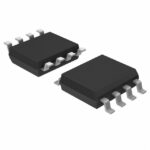 PBSS4021SPN,115
The activity of extra discounts on wholesale prices is in full swing…
Please fill in your contact information and we will send you the latest wholesale price list.






