 ChipApex | Global Electronic Components Supplier

SEARCH
Search Product
Search Post
— IC芯片 | 连接器 | 传感器 | 被动器件 —
Search productSearch post
— IC芯片 | 连接器 | 传感器 | 被动器件 —
Consult the customer manager about the wholesale price.
consultation hotline:86-132-6715-2157
email:[email protected]
Contact the product manager for consultation. One-stop consultation is available.
Do you want a lower wholesale price? Please send us your inquiry and we will reply immediately.
The PHC21025 is a complementary intermediate level N-channel and P-channel enhancement mode Field-Effect Transistor (FET) utilizing vertical D-MOS technology. It features a drain-source voltage of 30 V for both channels, with continuous drain currents of 3.5 A (N-channel) and -2.3 A (P-channel). The device offers low on-state resistance, typically 0.08 Ω for the N-channel and 0.22 Ω for the P-channel at 25 °C. Packaged in an SO8 plastic small outline package (SOT96-1), it supports a junction temperature up to 150 °C and total power dissipation of 1 W at 25 °C ambient.
Verify the specific ordering suffix against current distributor catalogs to ensure correct packaging configuration. Confirm that the component meets the required industrial or consumer application standards as automotive qualification is not indicated. Review the latest datasheet revision for any updates to thermal derating curves or absolute maximum ratings before finalizing design specifications.
Select this complementary pair for circuits requiring matched N-channel and P-channel switching performance within a single package. Ensure the gate drive voltage aligns with the specified thresholds for optimal RDSon performance. Consider the thermal resistance from junction to solder point when designing PCB layouts to maintain operation within the 150 °C junction temperature limit under expected load conditions.
This component belongs to NXP's portfolio of complementary MOSFETs designed for general-purpose switching applications. It utilizes vertical D-MOS technology to achieve efficient power handling in a compact SO8 package. The device is intended for computing, communications, consumer, and industrial sectors where space-saving complementary pairs are beneficial.
Publicly confirmed substitute part numbers are not available in the provided documentation.
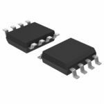 PHC21025,118

The activity of extra discounts on wholesale prices is in full swing…
Please fill in your contact information and we will send you the latest wholesale price list.





