 ChipApex | Global Electronic Components Supplier

SEARCH
Search Product
Search Post
— IC芯片 | 连接器 | 传感器 | 被动器件 —
Search productSearch post
— IC芯片 | 连接器 | 传感器 | 被动器件 —
Consult the customer manager about the wholesale price.
consultation hotline:86-132-6715-2157
email:[email protected]
Contact the product manager for consultation. One-stop consultation is available.
Do you want a lower wholesale price? Please send us your inquiry and we will reply immediately.
The PHKD3NQ10T is a dual standard level N-channel enhancement mode Field-Effect Transistor utilizing TrenchMOS technology. It features a 100 V drain-source voltage rating and a maximum continuous drain current of 3 A per channel at 25 °C. The device exhibits a typical drain-source on-state resistance of 90 mΩ at VGS = 10 V and ID = 1.5 A. Total power dissipation reaches 2 W at 25 °C, with a peak pulsed drain current capability of 12 A. The component operates within a junction temperature range of -65 °C to 150 °C and is housed in an SO8 plastic small outline package.
Verify the specific ordering suffix against official Nexperia documentation to confirm package variant and reel specifications. Confirm that the product status remains active as manufacturing schedules may change. Ensure compliance with RoHS directives and check for any regional export control classifications applicable to this semiconductor component before finalizing procurement orders.
Select this component for circuits requiring dual N-channel isolation in a compact footprint. Evaluate thermal management requirements based on the specified junction-to-ambient thermal resistance values under surface mount conditions. Consider the gate charge parameters when designing drive circuits for optimal switching performance and efficiency in power conversion topologies.
This device belongs to the Nexperia TrenchMOS family of standard level FETs. It integrates two independent N-channel MOSFETs into a single SO8 package. The technology focuses on reducing conduction losses while maintaining fast switching speeds. This integration supports space-constrained designs in computing, communications, consumer electronics, and industrial equipment.
Consult official Nexperia cross-reference lists for verified substitutes. Ensure replacement parts match the SO8 package dimensions and pinout configuration. Verify that alternative components meet or exceed the 100 V breakdown voltage and 3 A current ratings required for the application.
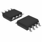 PHKD3NQ10T,518

The activity of extra discounts on wholesale prices is in full swing…
Please fill in your contact information and we will send you the latest wholesale price list.





