 ChipApex | Global Electronic Components Supplier

SEARCH
Search Product
Search Post
— IC芯片 | 连接器 | 传感器 | 被动器件 —
Search productSearch post
— IC芯片 | 连接器 | 传感器 | 被动器件 —
Consult the customer manager about the wholesale price.
consultation hotline:86-132-6715-2157
email:[email protected]
Contact the product manager for consultation. One-stop consultation is available.
Do you want a lower wholesale price? Please send us your inquiry and we will reply immediately.
The PJS6602_S2_00001 is a complementary enhancement mode MOSFET manufactured by Panjit International Inc. in an SOT-23 6L package. The N-channel device supports a drain-source voltage of 20V and continuous current of 5.2A, with a maximum on-resistance of 36mΩ at VGS=4.5V. The P-channel counterpart handles -20V and -3.4A, featuring a maximum on-resistance of 82mΩ at VGS=-4.5V. Both channels operate within a junction temperature range of -55°C to 150°C and are designed for switch load and PWM applications.
Verify the specific ordering suffix against official documentation to confirm packaging details. The _S2 variant indicates a 10K pcs / 13” reel configuration. Ensure compliance with Halogen-free and RoHS requirements as stated in the datasheet. Confirm that the component lot number matches tracking requirements for quality assurance purposes.
Select this component for low-voltage switching environments requiring complementary N-P channel pairs. Evaluate thermal resistance and power dissipation limits relative to ambient operating conditions. Verify gate drive voltages align with the specified thresholds for optimal on-state performance. Consider package limitations when determining maximum pulsed current capabilities.
This part belongs to the PJS6602 series of 20V complementary enhancement mode MOSFETs. It shares core electrical characteristics with other variants in the family, such as the _S1 version, differing primarily in reel size and packing quantity. The SC2 marking identifies the specific manufacturing batch and revision.
Direct substitutes must match the 20V rating, SOT-23 6L package, and complementary N/P structure. Verify pinout compatibility and thermal resistance values before implementation.
The maximum continuous drain current (ID) for the N-channel is 5.2A.
No, the manufacturer explicitly disclaims authorization for use in medical instruments or life-saving equipment.
The typical total gate charge (Qg) is 4.1nC under test conditions of VDS=10V, ID=5.2A, and VGS=4.5V.
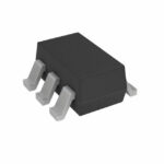 PJS6602_S2_00001

The activity of extra discounts on wholesale prices is in full swing…
Please fill in your contact information and we will send you the latest wholesale price list.





