 ChipApex | Global Electronic Components Supplier

SEARCH
Search Product
Search Post
— IC芯片 | 连接器 | 传感器 | 被动器件 —
Search productSearch post
— IC芯片 | 连接器 | 传感器 | 被动器件 —
Consult the customer manager about the wholesale price.
consultation hotline:86-132-6715-2157
email:[email protected]
Contact the product manager for consultation. One-stop consultation is available.
Do you want a lower wholesale price? Please send us your inquiry and we will reply immediately.
The PJS6832_S2_00001 is a 30V N-Channel Enhancement Mode MOSFET manufactured by Panjit International Inc. It utilizes advanced trench process technology and features ESD protection rated at 2kV HBM. The device operates within a junction temperature range of -55°C to +150°C. Key electrical parameters include a drain-source breakdown voltage (BVDSS) of 30V, continuous drain current (ID) of 1.6A, and pulsed drain current (IDM) of 6.4A. On-state resistance (RDS(on)) is specified as a maximum of 200mΩ at VGS=4.5V/ID=1.6A, 270mΩ at VGS=2.5V/ID=1.1A, and 570mΩ at VGS=1.8V/ID=0.2A. Total gate charge (Qg) is typically 1.5nC under standard test conditions.
Verify the specific ordering suffix against official documentation to confirm packaging details. The S2 variant corresponds to a 10K pcs / 13” reel packing code. Ensure compliance with RoHS 2.0 and IEC 61249 green molding compound standards during procurement. Confirm lot number availability for tracking purposes when placing orders.
Select this component based on required voltage and current ratings relative to the application circuit. Evaluate RDS(on) specifications across different gate drive voltages (1.8V, 2.5V, 4.5V) to ensure compatibility with the control logic. Consider thermal resistance and power dissipation limits for proper heat management in the final design.
This part belongs to the PJS6832 series of 30V N-Channel Enhancement Mode MOSFETs. The S2_00001 suffix specifically denotes the 10K pcs / 13” reel packing configuration. Other variants like S1_00001 exist with different reel sizes but share identical electrical characteristics and package type.
Publicly confirmed substitute part numbers are not available in the provided datasheet or source material. Consult manufacturer catalogs for direct replacements if necessary.
The device features ESD protection rated at 2KV HBM.
The maximum pulsed drain current (IDM) is 6.4 A.
Yes, it is lead-free in compliance with EU RoHS 2.0 and uses green molding compound as per IEC 61249 standard.
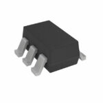 PJS6832_S2_00001

The activity of extra discounts on wholesale prices is in full swing…
Please fill in your contact information and we will send you the latest wholesale price list.





