 ChipApex | Global Electronic Components Supplier

SEARCH
Search Product
Search Post
— IC芯片 | 连接器 | 传感器 | 被动器件 —
Search productSearch post
— IC芯片 | 连接器 | 传感器 | 被动器件 —
Consult the customer manager about the wholesale price.
consultation hotline:86-132-6715-2157
email:[email protected]
Contact the product manager for consultation. One-stop consultation is available.
Do you want a lower wholesale price? Please send us your inquiry and we will reply immediately.
The PJX8808_R1_00001 is a dual N-Channel Enhancement Mode MOSFET manufactured by Panjit International Inc. in an SOT-563 package. It features a Drain-Source Voltage (VDS) of 20 V and a Continuous Drain Current (ID) of 500 mA. The device utilizes advanced trench process technology to achieve low on-state resistance, with RDS(on) values ranging from 310 mΩ at VGS=4.5V to 710 mΩ at VGS=1.2V. Key electrical parameters include a Gate Threshold Voltage (VGS(th)) of 0.64 V typical, total gate charge (Qg) of 1.4 nC, and power dissipation of 300 mW at 25°C ambient temperature.
Verify the component authenticity by checking the marking code X08 on the SOT-563 package against official datasheets. Confirm compliance with EU RoHS 2.0 standards and IEC 61249 green molding compound requirements during incoming inspection. Ensure storage conditions maintain moisture sensitivity level integrity prior to soldering.
Select this component for low-voltage switching designs requiring 20V breakdown and 500mA continuous current handling. Consider the thermal resistance of 417 °C/W when designing heat dissipation strategies. Verify that the drive voltage meets the minimum threshold requirements for the desired on-state resistance performance levels.
This part belongs to the Panjit MOSFET portfolio, specifically designed as a dual N-Channel enhancement mode device. It is housed in a compact SOT-563 surface-mount package suitable for space-constrained PCB layouts. The product line emphasizes energy efficiency through low on-resistance and fast switching characteristics.
No publicly confirmed substitute part numbers are documented in the provided source material. Cross-referencing requires matching VDS, ID, RDS(on), and package type specifications independently.
The maximum pulsed drain current (IDM) is 1000 mA.
The gate threshold voltage (VGS(th)) has a minimum of 0.3 V, a typical value of 0.64 V, and a maximum of 0.9 V under test conditions of VDS=VGS and ID=250uA.
The maximum Drain-Source Diode Forward Voltage (VSD) is 1.3 V when the current IS is 500 mA and VGS is 0 V.
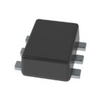 PJX8808_R1_00001

The activity of extra discounts on wholesale prices is in full swing…
Please fill in your contact information and we will send you the latest wholesale price list.





