 ChipApex | Global Electronic Components Supplier
SEARCH
Search Product
Search Post
— IC芯片 | 连接器 | 传感器 | 被动器件 —
Search productSearch post
— IC芯片 | 连接器 | 传感器 | 被动器件 —
Consult the customer manager about the wholesale price.
consultation hotline:86-132-6715-2157
email:[email protected]
Contact the product manager for consultation. One-stop consultation is available.
Do you want a lower wholesale price? Please send us your inquiry and we will reply immediately.
The PMBFJ620,115 is a dual N-channel symmetrical junction field-effect transistor housed in a SOT363 plastic surface-mounted package. It integrates two independent FETs within a single compact footprint to minimize board space and component count. The device supports a drain-source voltage of ±25 V and offers low noise performance with high gain characteristics. Key electrical parameters include a total power dissipation of 190 mW at temperatures up to 90 °C, a typical forward transfer admittance of 10 mS, and a maximum gate-source cut-off voltage of -6.5 V.
Verify the specific ordering suffix matches the required manufacturing origin (Hong Kong, Malaysia, or China) as indicated by the marking code. Confirm the package version corresponds to the SOT363 specification. Ensure handling procedures adhere to ESD sensitivity standards during assembly. Cross-reference the latest product data sheet revision to confirm current status and any potential parameter updates before finalizing procurement specifications.
Select this component when a dual N-channel JFET configuration is required in a minimal footprint. The symmetrical design simplifies circuit layout by allowing flexible pin usage for source and drain connections. Consider the thermal resistance limits and power dissipation constraints relative to the operating ambient temperature. Verify that the low noise and high gain attributes align with the specific requirements of the target RF or audio application.
This discrete semiconductor component belongs to NXP's portfolio of general-purpose junction field-effect transistors. It is designed for surface-mount technology integration, supporting automated assembly processes. The SOT363 package provides a standardized form factor compatible with various PCB layouts. This part serves as a fundamental building block for analog and RF circuits requiring dual matched transistor pairs.
Public confirmed substitute part numbers are not available in the provided documentation. Consult official NXP resources for equivalent products if direct replacement is necessary.
The maximum drain-source voltage (VDS) is ±25 V per FET.
The SOT363 package contains six leads.
Yes, the device is sensitive to ElectroStatic Discharge (ESD), and appropriate handling precautions must be observed.
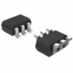 PMBFJ620,115
The activity of extra discounts on wholesale prices is in full swing…
Please fill in your contact information and we will send you the latest wholesale price list.






