ChipApex | Global Electronic Components Supplier

SEARCH
Search Product
Search Post
— IC芯片 | 连接器 | 传感器 | 被动器件 —
Search productSearch post
— IC芯片 | 连接器 | 传感器 | 被动器件 —
Consult the customer manager about the wholesale price.
consultation hotline:86-132-6715-2157
email:[email protected]
Contact the product manager for consultation. One-stop consultation is available.
Do you want a lower wholesale price? Please send us your inquiry and we will reply immediately.
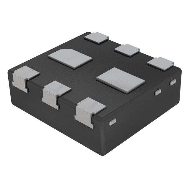
The PMCXB900UE is a complementary N/P-channel enhancement mode Field-Effect Transistor utilizing Trench MOSFET technology. It features a leadless DFN1010B-6 (SOT1216) package measuring 1.1 x 1.0 x 0.37 mm. The N-channel device has a drain-source voltage of 20 V and on-state resistance of 470 mΩ at VGS=4.5 V, ID=600 mA. The P-channel device has a drain-source voltage of -20 V and on-state resistance of 1.02 Ω at VGS=-4.5 V, ID=-500 mA. Both channels exhibit a low threshold voltage of 0.7 V typical and ESD protection exceeding 1 kV HBM.
Verify the specific ordering suffix against the manufacturer's current catalog to ensure correct packaging and marking codes. Confirm that the DFN1010B-6 footprint matches your PCB design guidelines. Check for any recent revision history updates that may affect thermal or electrical specifications. Ensure compatibility with your assembly process requirements for this leadless package type.
Select this component when space constraints require an ultra-thin, leadless surface-mount solution. The complementary N/P configuration simplifies circuit design for level shifting and driver applications. Consider the low threshold voltage for efficient operation in battery-powered systems. Evaluate thermal dissipation capabilities based on the specific PCB copper area available for the drain mounting pad.
This device belongs to Nexperia's portfolio of small-signal MOSFETs designed for high-density electronics. The DFN1010B-6 package is part of the SOT1216 family, offering minimal board space consumption. It targets consumer electronics and portable devices where size and power efficiency are critical design parameters.
No public confirmed substitute part numbers are documented in the provided datasheet.
 PMCXB900UEZ

The activity of extra discounts on wholesale prices is in full swing…
Please fill in your contact information and we will send you the latest wholesale price list.