ChipApex | Global Electronic Components Supplier

SEARCH
Search Product
Search Post
— IC芯片 | 连接器 | 传感器 | 被动器件 —
Search productSearch post
— IC芯片 | 连接器 | 传感器 | 被动器件 —
Consult the customer manager about the wholesale price.
consultation hotline:86-132-6715-2157
email:[email protected]
Contact the product manager for consultation. One-stop consultation is available.
Do you want a lower wholesale price? Please send us your inquiry and we will reply immediately.
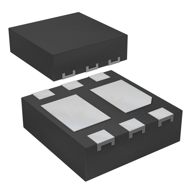
The PMDPB55XP,115 is a dual P-channel enhancement mode Field-Effect Transistor utilizing Trench MOSFET technology. It features a DFN2020-6 (SOT1118) leadless package measuring 2 x 2 x 0.65 mm with an exposed drain pad for thermal conduction. Key electrical parameters include a drain-source voltage of 20 V, continuous drain current of 4.5 A, and on-state resistance of 55 mΩ at VGS = -4.5 V. The device operates within a junction temperature range of -55 °C to +150 °C.
Verify the complete part number including the suffix
Select this component for applications requiring compact dual P-channel switching solutions. The low on-state resistance supports efficient power handling in small form factors. Ensure gate drive voltages remain within the specified limits to maintain optimal performance and reliability during operation.
This device belongs to Nexperia's portfolio of Trench MOSFETs designed for high-efficiency power management. The DFN2020-6 package offers a leadless surface-mount solution suitable for automated assembly processes. It serves as a compact alternative to traditional through-hole or larger surface-mount packages in space-constrained electronic designs.
No public confirmed substitute part numbers are available in the provided documentation.
The maximum junction temperature is +150 °C.
No, unless expressly stated otherwise, the product is not suitable for automotive use and is not qualified according to automotive testing requirements.
The component uses a DFN2020-6 (SOT1118) plastic thermal enhanced ultra thin small outline package with no leads.
 PMDPB55XP,115

The activity of extra discounts on wholesale prices is in full swing…
Please fill in your contact information and we will send you the latest wholesale price list.