ChipApex | Global Electronic Components Supplier

SEARCH
Search Product
Search Post
— IC芯片 | 连接器 | 传感器 | 被动器件 —
Search productSearch post
— IC芯片 | 连接器 | 传感器 | 被动器件 —
Consult the customer manager about the wholesale price.
consultation hotline:86-132-6715-2157
email:[email protected]
Contact the product manager for consultation. One-stop consultation is available.
Do you want a lower wholesale price? Please send us your inquiry and we will reply immediately.
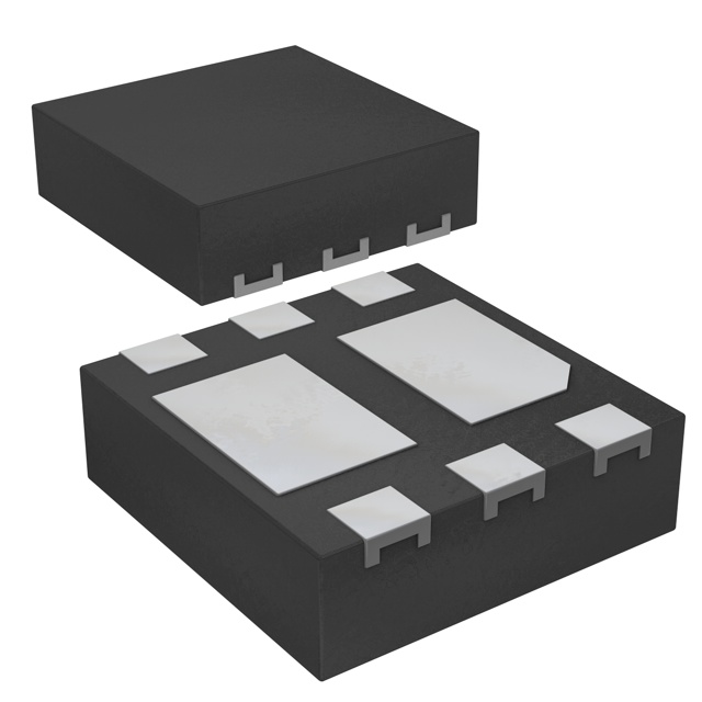
The PMDPB65UP,115 is a dual small-signal P-channel enhancement mode Field-Effect Transistor manufactured by Nexperia. It utilizes Trench MOSFET technology within an ultra-thin SOT1118 (HUSON6) leadless plastic package measuring 2 × 2 × 0.65 mm. The device features an exposed drain pad for thermal management and provides 1 kV ESD protection. Key electrical parameters include a drain-source voltage of 20 V, continuous drain current of 3.5 A per transistor, and a maximum on-state resistance of 70 mΩ at VGS = -4.5 V. It operates with junction temperatures up to 150 °C.
Verify the component manufacturer as Nexperia, which acquired the former NXP Standard Product business in February 2017. Confirm the package type is SOT1118 (HUSON6) and check for RoHS compliance status. Ensure the ordering suffix matches the specific reel or cut tape configuration required for assembly processes.
Select this component for applications requiring dual P-channel switching in space-constrained designs. The 20 V rating suits low-voltage systems, while the 1.8 V RDSon capability allows compatibility with low-voltage logic gates. Verify that the PCB footprint accommodates the 6 cm² drain mounting pad requirement for optimal thermal performance if operating near maximum current limits.
This part belongs to the PMDPB series of dual small-signal P-channel MOSFETs from Nexperia. It is designed for high-efficiency power management in compact consumer electronics and industrial control systems. The HUSON6 package represents a transition toward leadless, thermally enhanced surface-mount technologies for improved heat dissipation in dense layouts.
Direct substitutes must match the 20 V/3.5 A dual P-channel specification and SOT1118 package. Check datasheets for equivalent RDSon values and pinout configurations to ensure interchangeability without circuit redesign.
The device offers 1 kV ESD protection according to the Human Body Model (HBM).
Lower gate-source voltages increase RDSon; it is rated at 70 mΩ max at -4.5 V but rises to 150 mΩ max at -1.8 V.
For optimal thermal performance, a drain mounting pad of 6 cm² on an FR4 PCB is recommended.
 PMDPB65UP,115

The activity of extra discounts on wholesale prices is in full swing…
Please fill in your contact information and we will send you the latest wholesale price list.