ChipApex | Global Electronic Components Supplier

SEARCH
Search Product
Search Post
— IC芯片 | 连接器 | 传感器 | 被动器件 —
Search productSearch post
— IC芯片 | 连接器 | 传感器 | 被动器件 —
Consult the customer manager about the wholesale price.
consultation hotline:86-132-6715-2157
email:[email protected]
Contact the product manager for consultation. One-stop consultation is available.
Do you want a lower wholesale price? Please send us your inquiry and we will reply immediately.
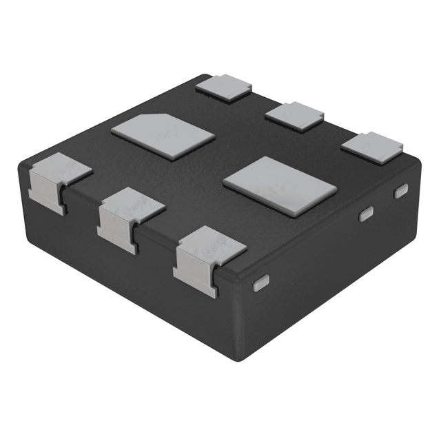
The PMDXB590UPE is a dual P-channel enhancement mode Field-Effect Transistor utilizing Trench MOSFET technology. It is housed in a leadless DFN1010B-6 (SOT1216) plastic package with dimensions of 1.1 mm x 1.0 mm x 0.37 mm. The device supports a drain-source voltage of -20 V and a gate-source voltage range of -8 V to 8 V. At VGS = -4.5 V, the typical drain current is -0.57 A (Tamb) or -2.3 A (Tsp), with a maximum on-state resistance of 770 mΩ at 25 °C.
Verify the specific ordering suffix 'UPE' against the manufacturer's latest documentation to confirm the exact reel configuration and marking code. Ensure the design accommodates the thermal characteristics defined for the DFN1010B-6 package, specifically regarding junction-to-ambient resistance values under different PCB mounting conditions.
Select this component when a compact dual P-channel solution is required for low-voltage applications. The ultra-thin profile suits space-constrained designs. Evaluate the on-state resistance requirements against the specified limits at operating temperatures to ensure adequate current handling capabilities within the thermal constraints of the target PCB footprint.
This part belongs to Nexperia's portfolio of small-signal MOSFETs designed for portable electronics and general-purpose switching. The DFN1010B-6 package provides a balance between thermal dissipation and minimal board area usage compared to traditional leaded packages.
Check for direct substitutes such as the PMDXB590UNEZ variant, ensuring pinout compatibility and identical electrical specifications before substitution.
The device supports a peak drain current of -9.2 A for single pulses with a duration of 10 µs or less.
The RDSon increases significantly at higher temperatures; it rises from a typical 590 mΩ at 25 °C to approximately 890 mΩ at 150 °C under standard test conditions.
 PMDXB590UPEZ

The activity of extra discounts on wholesale prices is in full swing…
Please fill in your contact information and we will send you the latest wholesale price list.