 ChipApex | Global Electronic Components Supplier

SEARCH
Search Product
Search Post
— IC芯片 | 连接器 | 传感器 | 被动器件 —
Search productSearch post
— IC芯片 | 连接器 | 传感器 | 被动器件 —
Consult the customer manager about the wholesale price.
consultation hotline:86-132-6715-2157
email:[email protected]
Contact the product manager for consultation. One-stop consultation is available.
Do you want a lower wholesale price? Please send us your inquiry and we will reply immediately.
The PMWD16UN is a dual N-channel enhancement mode Field-Effect Transistor (FET) utilizing TrenchMOS technology. It features an ultra-low threshold voltage and fast switching capabilities within a plastic surface-mount package. The device supports a drain-source voltage of 20 V and continuous drain currents up to 9.9 A at 25 °C. Key electrical parameters include a maximum on-state resistance of 19 mΩ at VGS = 4.5 V and a total power dissipation of 3.1 W. The component is housed in an 8-lead TSSOP package (SOT530-1).
Verify the specific ordering information against the manufacturer's current documentation before procurement. Confirm that the SOT530-1 package version matches design requirements. Ensure thermal management strategies align with the specified junction-to-solder point thermal resistance limits provided in the datasheet.
Select this component when a compact dual FET solution with low RDS(on) is required for portable or battery-powered designs. Evaluate the 20 V breakdown voltage and 9.9 A current rating against peak load demands. Consider the TSSOP8 footprint constraints and verify compatibility with automated assembly processes for thin shrink small outline packages.
This component belongs to the family of dual N-channel enhancement mode field-effect transistors manufactured by Philips Semiconductors, now part of NXP USA Inc. It utilizes proprietary TrenchMOS technology to achieve low on-resistance and fast switching speeds within a compact plastic package designed for surface mounting applications.
Consult official replacement lists for verified substitutes. Cross-reference pinout configurations and electrical ratings carefully to ensure functional equivalence without redesigning the printed circuit board layout.
The maximum continuous drain current is 9.9 A at a solder point temperature of 25 °C and a gate-source voltage of 4.5 V.
The PMWD16UN uses a TSSOP8 plastic thin shrink small outline package, identified as SOT530-1, featuring 8 leads with a body width of 4.4 mm.
The typical gate-source threshold voltage is 0.7 V, measured with a drain current of 1 mA and VDS equal to VGS.
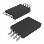 PMWD16UN,518

The activity of extra discounts on wholesale prices is in full swing…
Please fill in your contact information and we will send you the latest wholesale price list.





