ChipApex | Global Electronic Components Supplier

SEARCH
Search Product
Search Post
— IC芯片 | 连接器 | 传感器 | 被动器件 —
Search productSearch post
— IC芯片 | 连接器 | 传感器 | 被动器件 —
Consult the customer manager about the wholesale price.
consultation hotline:86-132-6715-2157
email:[email protected]
Contact the product manager for consultation. One-stop consultation is available.
Do you want a lower wholesale price? Please send us your inquiry and we will reply immediately.
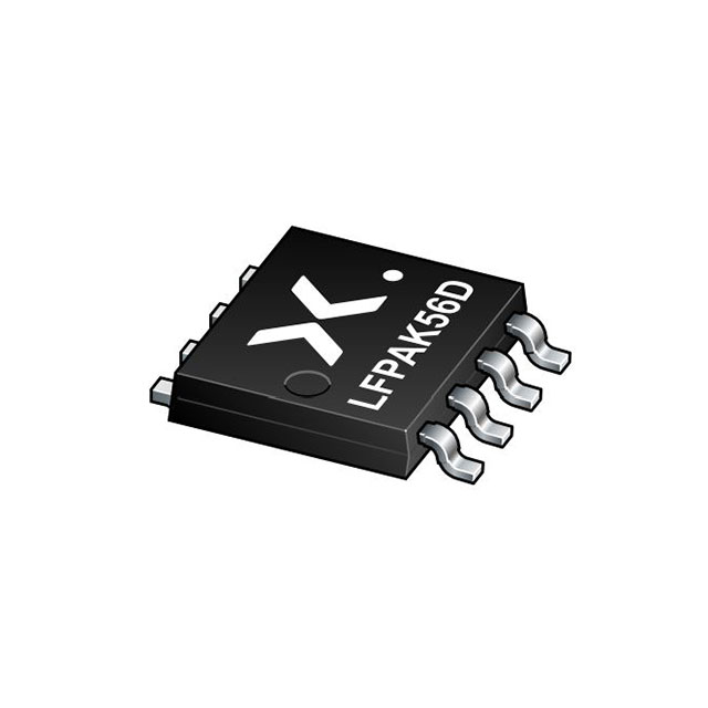
The PSMN028-100HS is a dual standard level N-channel MOSFET in an LFPAK56D (Dual Power-SO8) package using TrenchMOS technology. It features a drain-source voltage of 100 V and a typical on-state resistance of 27.5 mΩ at 25 °C. The device supports a continuous drain current of 29 A and a peak pulsed current of 116 A. Total power dissipation reaches 64 W with a junction temperature range up to 175 °C. Key dynamic parameters include a total gate charge of 34 nC and a non-repetitive avalanche energy rating of 67 mJ.
Verify the specific ordering suffix and marking code against the official Nexperia datasheet before procurement. Confirm that the LFPAK56D package variant matches the required footprint for your PCB design. Ensure the component status is listed as production data rather than preliminary or objective development stages. Check for any recent longevity program updates regarding expected order availability times.
Select this component when a dual N-channel configuration is required within a compact surface-mount form factor. The standard level gate drive requires a 10 V gate-source voltage for optimal performance. Consider the thermal resistance characteristics and mounting base temperature limits for heat dissipation planning. Evaluate the avalanche ruggedness if the application involves inductive switching loads.
This dual MOSFET utilizes Nexperia's TrenchMOS technology to achieve low conduction losses. The LFPAK56D package provides enhanced thermal performance compared to traditional plastic packages. It is designed for industrial, communications, and domestic equipment applications requiring robust switching capabilities.
No public confirmed substitute part numbers are available in the provided documentation.
 PSMN028-100HSX

The activity of extra discounts on wholesale prices is in full swing…
Please fill in your contact information and we will send you the latest wholesale price list.