ChipApex | Global Electronic Components Supplier

SEARCH
Search Product
Search Post
— IC芯片 | 连接器 | 传感器 | 被动器件 —
Search productSearch post
— IC芯片 | 连接器 | 传感器 | 被动器件 —
Consult the customer manager about the wholesale price.
consultation hotline:86-132-6715-2157
email:[email protected]
Contact the product manager for consultation. One-stop consultation is available.
Do you want a lower wholesale price? Please send us your inquiry and we will reply immediately.
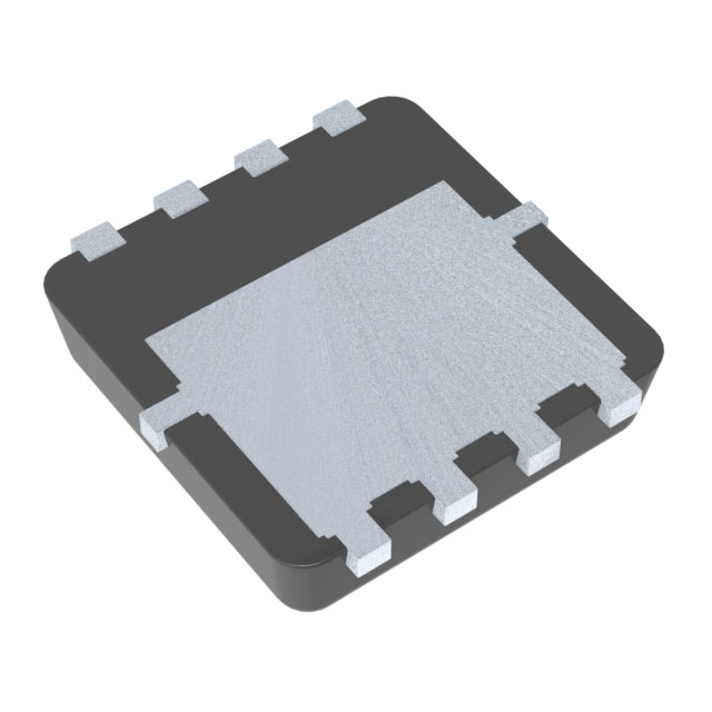
PXP010-20QXJ is listed in the Single FETs, MOSFETs range at ChipApex. The manufacturer field lists Nexperia USA Inc.. Its product description is PXP010-20QX/SOT8002/MLPAK33. Review the specifications below when checking this part for your BOM.
The PXP010-20QX is a 20 V, P-channel enhancement mode Field-Effect Transistor utilizing Trench MOSFET technology. It is housed in an MLPAK33 (SOT8002) surface-mounted plastic package with a 3.3 x 3.3 mm footprint. The device features a low threshold voltage and supports a drain-source voltage of -20 V. At 25 °C, the on-state resistance is typically 8.4 mΩ at VGS = -4.5 V and ID = -10.6 A. The maximum continuous drain current reaches -17.1 A under specific conditions, with a peak current capability of -63 A for single pulses.
Verify the exact part number against the official Nexperia datasheet to ensure compatibility with your design requirements. Confirm that the MLPAK33 package dimensions and pinout match your PCB layout specifications. Check the most recent product data sheet for any updates to electrical characteristics or thermal limits before finalizing component selection.
Select this component for applications requiring a compact P-channel solution with high current handling capabilities. The MLPAK33 package offers a small footprint suitable for space-constrained designs. Ensure the gate drive voltage meets the minimum requirements for optimal RDS(on) performance. Consider the thermal resistance values when designing heat dissipation strategies for high-power applications.
This device belongs to Nexperia's portfolio of power MOSFETs designed for efficient power management. The MLPAK33 package represents a thermal-enhanced surface-mount option, providing improved heat dissipation compared to standard packages of similar size. It is intended for use in modern electronic systems where size and efficiency are critical factors.
No public confirmed substitute part numbers are available in the provided documentation.
The maximum drain-source voltage (VDS) is rated at -20 V.
The typical drain-source on-state resistance (RDSon) is 8.4 mΩ when VGS is -4.5 V and ID is -10.6 A at 25 °C.
Explore related parts through FETs, MOSFETs, Transistors, Discrete Semiconductor Products, all product categories.
 PXP010-20QXJ

The activity of extra discounts on wholesale prices is in full swing…
Please fill in your contact information and we will send you the latest wholesale price list.