ChipApex | Global Electronic Components Supplier
SEARCH
Search Product
Search Post
— IC芯片 | 连接器 | 传感器 | 被动器件 —
Search productSearch post
— IC芯片 | 连接器 | 传感器 | 被动器件 —
Consult the customer manager about the wholesale price.
consultation hotline:86-132-6715-2157
email:[email protected]
Contact the product manager for consultation. One-stop consultation is available.
Do you want a lower wholesale price? Please send us your inquiry and we will reply immediately.
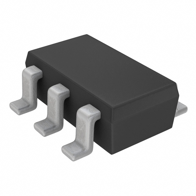
The QS6M3TR is a dual-channel MOSFET containing one N-channel and one P-channel transistor in a TSMT6 (SOT-457T) surface-mount package. It features a low on-resistance design optimized for 2.5V drive applications, with typical RDS(on) values of 0.26Ω at VGS=2.5V for both channels. The device includes built-in gate-source protection diodes and body diodes. Key electrical ratings include a drain-source voltage of ±30V, continuous drain current of ±1.5A, and total power dissipation of 1.25W. Total gate charge is typically 1.6nC for the N-channel and 3.0nC for the P-channel.
Verify the specific ordering suffix to confirm tape-and-reel packaging quantities. Ensure compatibility with RoHS standards if required by your manufacturing process. Confirm that the component status aligns with your production timeline needs before finalizing orders.
Select this component when a complementary N/P pair is needed in a single small footprint. The 2.5V drive capability makes it suitable for low-voltage logic interfaces. Verify thermal management requirements as the total power dissipation is limited to 1.25W.
This part belongs to ROHM's small switching transistor series designed for compact power management solutions. The TSMT6 package allows for high-density PCB layouts. It serves as a complementary pair solution for bridge drivers or load switches where space is constrained.
QS6M4TR
The typical static drain-source on-state resistance is 0.26Ω for both the N-channel and P-channel at VGS = 2.5V.
Yes, the device features built-in gate-source protection diodes to enhance reliability against electrostatic discharge.
The absolute maximum drain-source voltage (VDSS) is rated at ±30V for both channels.
 QS6M3TR
The activity of extra discounts on wholesale prices is in full swing…
Please fill in your contact information and we will send you the latest wholesale price list.