 ChipApex | Global Electronic Components Supplier
SEARCH
Search Product
Search Post
— IC芯片 | 连接器 | 传感器 | 被动器件 —
Search productSearch post
— IC芯片 | 连接器 | 传感器 | 被动器件 —
Consult the customer manager about the wholesale price.
consultation hotline:86-132-6715-2157
email:[email protected]
Contact the product manager for consultation. One-stop consultation is available.
Do you want a lower wholesale price? Please send us your inquiry and we will reply immediately.
The Vishay Siliconix SI1900DL-T1-GE3 is a dual N-channel enhancement mode MOSFET utilizing TrenchFET technology. It features a 30 V drain-source voltage rating and operates within a junction temperature range of -55 °C to +150 °C. The device provides a maximum continuous drain current of 0.63 A at 25 °C, with an on-state resistance of 0.480 Ω at VGS = 10 V and 0.700 Ω at VGS = 4.5 V. Packaged in a surface-mount SOT-363 (SC-70) housing, it offers a total gate charge of 1.4 nC and a maximum power dissipation of 0.30 W.
Verify the complete part number including the suffix to confirm halogen-free status and lead-free composition. Confirm that the SOT-363 footprint matches the recommended pad dimensions specified in Application Note 826. Ensure procurement channels provide original manufacturer documentation to validate RoHS compliance and traceability requirements.
Select this component when a dual N-channel topology is required in a minimal footprint. Evaluate thermal constraints carefully as the maximum power dissipation is limited to 0.30 W. Verify that the 30 V breakdown voltage aligns with the system's supply rails and ensure the gate drive voltage supports the specified RDS(on) thresholds.
This component belongs to the Si1900 series of dual MOSFETs from Vishay Siliconix. It shares the SC-70 form factor with other small-signal variants but is distinguished by its specific 30 V rating and dual-channel architecture. The product line emphasizes low profile packaging suitable for high-density PCB layouts.
Direct replacements must match the SOT-363 pinout and electrical ratings. Verify that alternative dual N-channel MOSFETs maintain compatible VGS(th) levels and offer equivalent or lower RDS(on) values to ensure circuit performance parity without redesigning the thermal solution.
The maximum continuous drain current is 0.63 A at an ambient temperature of 25 °C, decreasing to 0.45 A at 85 °C.
Yes, it is compliant with the RoHS Directive 2002/95/EC and is defined as halogen-free according to IEC 61249-2-21.
The typical RDS(on) is 0.480 Ω at VGS = 10 V and increases to 0.700 Ω at VGS = 4.5 V under specified test conditions.
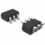 SI1900DL-T1-GE3
The activity of extra discounts on wholesale prices is in full swing…
Please fill in your contact information and we will send you the latest wholesale price list.





