 ChipApex | Global Electronic Components Supplier
SEARCH
Search Product
Search Post
— IC芯片 | 连接器 | 传感器 | 被动器件 —
Search productSearch post
— IC芯片 | 连接器 | 传感器 | 被动器件 —
Consult the customer manager about the wholesale price.
consultation hotline:86-132-6715-2157
email:[email protected]
Contact the product manager for consultation. One-stop consultation is available.
Do you want a lower wholesale price? Please send us your inquiry and we will reply immediately.
The SI3585CDV-T1-GE3 is a dual-channel MOSFET from Vishay Siliconix, integrating an N-channel and a P-channel device within a single TSOP-6 package. The N-channel component provides a maximum drain-source voltage of 20 V with a typical on-resistance of 0.058 Ω at a gate-source voltage of 4.5 V, supporting a continuous drain current of 3.9 A. The complementary P-channel unit shares the same 20 V rating but features a typical on-resistance of 0.195 Ω at -4.5 V, accommodating a continuous drain current of 2.1 A. Both channels utilize TrenchFET technology.
Verify the specific ordering suffix against official documentation to confirm lead-free and halogen-free compliance status. Confirm that the TSOP-6 package dimensions align with the recommended land pattern specifications provided by the manufacturer. Ensure that thermal management strategies account for the junction-to-ambient resistance ratings under steady-state conditions.
Select this component when a design requires matched N-type and P-type switching capabilities within a constrained footprint. Evaluate the on-resistance values at the intended operating gate voltages to ensure adequate efficiency. Consider the continuous and pulsed current limits relative to the expected load profile and ambient temperature conditions.
This part belongs to the Si3585CDV series of dual-channel MOSFETs manufactured by Vishay Siliconix. It is designed as a compact solution for applications requiring both high-side and low-side switching functions. The integration of complementary channels simplifies circuit topology compared to using discrete single-channel devices.
Direct pin-compatible replacements must maintain the TSOP-6 form factor and match the 20 V drain-source voltage rating. Verify that alternative components offer comparable on-resistance and current handling capabilities to ensure equivalent thermal and electrical performance.
The absolute maximum rating for the gate-source voltage (VGS) is ±12 V for both the N-channel and P-channel devices.
At a gate-source voltage of 4.5 V, the P-channel typical on-resistance is 0.195 Ω, which is higher than the N-channel typical on-resistance of 0.058 Ω.
The standard datasheet does not list AEC-Q101 qualification or automotive grade certification for this specific part number; verification of specific application requirements is necessary.
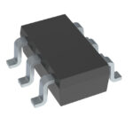 SI3585CDV-T1-GE3
The activity of extra discounts on wholesale prices is in full swing…
Please fill in your contact information and we will send you the latest wholesale price list.





