 ChipApex | Global Electronic Components Supplier
SEARCH
Search Product
Search Post
— IC芯片 | 连接器 | 传感器 | 被动器件 —
Search productSearch post
— IC芯片 | 连接器 | 传感器 | 被动器件 —
Consult the customer manager about the wholesale price.
consultation hotline:86-132-6715-2157
email:[email protected]
Contact the product manager for consultation. One-stop consultation is available.
Do you want a lower wholesale price? Please send us your inquiry and we will reply immediately.
The Vishay Siliconix SI4532CDY-T1-GE3 is a dual N- and P-channel enhancement-mode MOSFET in an SO-8 package. It utilizes TrenchFET technology for optimized performance. The N-channel device supports a drain-source voltage of 30 V with a maximum continuous drain current of 6.0 A at TC = 25 °C, featuring a typical on-resistance of 0.047 Ω at VGS = 10 V. The P-channel counterpart provides a 30 V rating and a maximum continuous drain current of -4.3 A at TC = 25 °C, with a typical on-resistance of 0.089 Ω at VGS = -10 V. Both channels are rated for a maximum power dissipation of 2.78 W at TC = 25 °C.
Verify the specific ordering suffix against official documentation to confirm compliance details. The GE3 designation indicates lead-free and halogen-free construction compliant with IEC 61249-2-21 standards. Ensure that the component meets RoHS Directive 2002/95/EC requirements for your intended application before finalizing procurement specifications.
Select this component when a compact dual-channel solution is required for low-voltage switching applications. The SO-8 package facilitates surface-mount assembly while providing adequate thermal management through the exposed drain pad. Evaluate the junction-to-ambient thermal resistance limits under your specific PCB layout conditions to ensure operation within the specified temperature range.
This part belongs to the Vishay Siliconix Si4532CDY series, which features isolated N- and P-channel MOSFETs in a single SO-8 package. The product line is designed for space-constrained designs requiring complementary channel configurations. The datasheet document number is 64805, revision S11-0652-Rev. B.
Consult the manufacturer's documentation for verified alternative part numbers or cross-reference options. Direct replacements must match the electrical ratings, pin configuration, and thermal characteristics of the original component.
The maximum pulsed drain current (IDM) for the N-channel is 24 A with a 10 µs pulse width.
Yes, the datasheet specifies 100% UIS (Unclamped Inductive Switching) testing. The single-pulse avalanche energy (EAS) is 2.5 mJ for the N-channel and 3.2 mJ for the P-channel at L = 0.1 mH.
The operating junction and storage temperature range (TJ, Tstg) is from -55 °C to +150 °C.
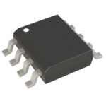 SI4532CDY-T1-GE3
The activity of extra discounts on wholesale prices is in full swing…
Please fill in your contact information and we will send you the latest wholesale price list.





