 ChipApex | Global Electronic Components Supplier
SEARCH
Search Product
Search Post
— IC芯片 | 连接器 | 传感器 | 被动器件 —
Search productSearch post
— IC芯片 | 连接器 | 传感器 | 被动器件 —
Consult the customer manager about the wholesale price.
consultation hotline:86-132-6715-2157
email:[email protected]
Contact the product manager for consultation. One-stop consultation is available.
Do you want a lower wholesale price? Please send us your inquiry and we will reply immediately.
The Vishay Siliconix SI4590DY-T1-GE3 is a dual N- and P-channel MOSFET utilizing TrenchFET technology, housed in an SO-8 package. The N-channel device offers a drain-source voltage of 100 V, with maximum on-resistance values of 0.057 Ω at VGS = 10 V and 0.072 Ω at VGS = 4.5 V. It supports a continuous drain current of 5.6 A at TJ = 150 °C and features a typical total gate charge of 11.5 nC at VGS = 10 V. The complementary P-channel MOSFET provides a -100 V breakdown voltage, with maximum on-resistance of 0.183 Ω at VGS = -10 V and 0.205 Ω at VGS = -4.5 V. It handles a continuous drain current of -3.4 A at TJ = 150 °C and has a typical total gate charge of 36 nC at VGS = -10 V.
Verify the component against the official Vishay datasheet (Document Number: 62937) to confirm technical specifications match design requirements. Ensure the ordering suffix corresponds to the required tape-and-reel packaging format. Confirm RoHS compliance status through manufacturer documentation prior to integration into production assemblies.
Select this component for applications requiring matched N- and P-channel pairs in a compact surface-mount footprint. Evaluate thermal management strategies based on junction-to-ambient resistance ratings. Verify that the gate drive voltage levels align with the specified thresholds for optimal on-resistance performance across the operating temperature range.
This part belongs to the Vishay Siliconix SI4 series of power MOSFETs. It utilizes the standard narrow SOIC (SO-8) JEDEC package format. The device integrates two distinct channel types to facilitate half-bridge or full-bridge topologies without requiring separate discrete components.
Consult the official Vishay replacement guide for verified cross-reference data. Do not substitute with generic equivalents without validating pinout compatibility and absolute maximum ratings against the original specifications.
The N-channel device supports a pulsed drain current of 30 A, while the P-channel device supports -20 A, both measured with a 100 μs pulse width.
Yes, the datasheet specifies single-pulse avalanche energy ratings of 1.3 mJ for the N-channel and 20 mJ for the P-channel devices.
The N-channel body diode has a typical reverse recovery time of 60 ns and charge of 55 nC. The P-channel body diode exhibits a typical reverse recovery time of 85 ns and charge of 190 nC.
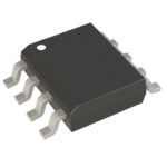 SI4590DY-T1-GE3
The activity of extra discounts on wholesale prices is in full swing…
Please fill in your contact information and we will send you the latest wholesale price list.





