ChipApex | Global Electronic Components Supplier
SEARCH
Search Product
Search Post
— IC芯片 | 连接器 | 传感器 | 被动器件 —
Search productSearch post
— IC芯片 | 连接器 | 传感器 | 被动器件 —
Consult the customer manager about the wholesale price.
consultation hotline:86-132-6715-2157
email:[email protected]
Contact the product manager for consultation. One-stop consultation is available.
Do you want a lower wholesale price? Please send us your inquiry and we will reply immediately.
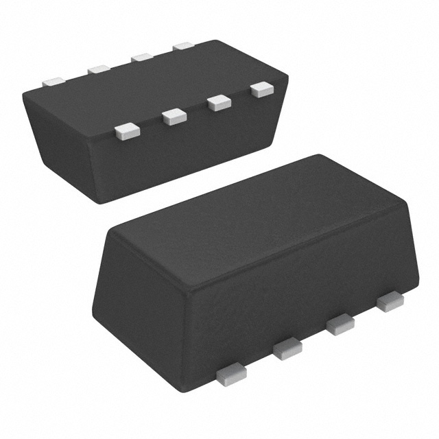
The Vishay Siliconix SI5513CDC-T1-E3 is a dual-channel MOSFET in the 1206-8 ChipFET package, integrating an N-channel and a P-channel device. The N-channel exhibits a drain-source voltage of 20 V, continuous drain current of 4 A at TC = 25 °C, and on-resistance of 0.055 Ω at VGS = 4.5 V. The P-channel provides -20 V breakdown, -3.7 A continuous current, and 0.150 Ω on-resistance at VGS = -4.5 V. Total gate charge reaches 4.2 nC for the N-channel and 5.6 nC for the P-channel. Thermal resistance from junction to foot is 40 °C/W maximum.
Verify component authenticity through authorized distributors or direct manufacturer channels. Confirm RoHS compliance and halogen-free status against current datasheet revisions. Validate lot traceability and date codes upon receipt. Ensure proper handling procedures are followed due to the leadless package design.
Evaluate thermal management requirements based on the specified junction-to-foot resistance. Verify that the PCB copper area supports the required power dissipation levels. Confirm gate drive voltages align with the specified thresholds for optimal on-state resistance. Consider the physical dimensions when designing the board layout.
This component belongs to the Vishay Siliconix Si5513CDC series, representing dual-channel power MOSFETs designed for space-constrained applications. It utilizes the 1206-8 ChipFET package, which offers thermal performance comparable to larger packages while maintaining a minimal footprint suitable for high-density circuit boards.
Si5513CDC-T1-GE3 (Lead-free and Halogen-free variant)
 SI5513CDC-T1-E3
The activity of extra discounts on wholesale prices is in full swing…
Please fill in your contact information and we will send you the latest wholesale price list.