ChipApex | Global Electronic Components Supplier
SEARCH
Search Product
Search Post
— IC芯片 | 连接器 | 传感器 | 被动器件 —
Search productSearch post
— IC芯片 | 连接器 | 传感器 | 被动器件 —
Consult the customer manager about the wholesale price.
consultation hotline:86-132-6715-2157
email:[email protected]
Contact the product manager for consultation. One-stop consultation is available.
Do you want a lower wholesale price? Please send us your inquiry and we will reply immediately.
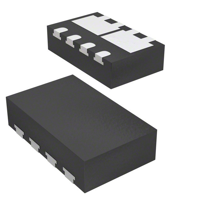
The Vishay Siliconix SI5944DU-T1-GE3 is a dual N-channel MOSFET utilizing TrenchFET technology. It features a 40 V drain-source voltage rating and operates within a -55 °C to +150 °C junction temperature range. The device is housed in a leadless PowerPAK ChipFET Dual 8 package with a 0.8 mm profile. At VGS = 10 V, the maximum on-state resistance is 0.112 Ω, supporting up to 6 A continuous drain current at TC = 25 °C. Total gate charge is typically 4.4 nC at VGS = 10 V.
Verify component authenticity through authorized distributors or direct manufacturer channels. Confirm the presence of the 'CC XXX' marking code and date lot traceability on the package. Ensure the ordering suffix matches the specified lead-free and halogen-free requirements. Validate datasheet revision B specifications against the delivered hardware batch.
Select this component for designs requiring dual N-channel isolation in a minimal space-constrained layout. Evaluate thermal management capabilities based on the 62 °C/W junction-to-ambient resistance when operating without heatsinking. Verify that the 40 V breakdown voltage accommodates system transients and that the 0.112 Ω on-resistance meets conduction loss targets at the intended load currents.
This part belongs to the Vishay Siliconix Si5944DU series of dual N-channel MOSFETs. It utilizes the PowerPAK ChipFET Dual 8 package, which is distinct from standard SOIC or QFN footprints due to its leadless design. The product line emphasizes low profile and enhanced thermal performance for portable electronics.
Consult official Vishay documentation for qualified alternatives. Cross-referencing requires matching the dual N-channel topology, 40 V rating, and PowerPAK ChipFET Dual 8 package dimensions to ensure mechanical compatibility.
The maximum operating junction temperature is 150 °C.
The PowerPAK ChipFET is a leadless package where the terminal ends are exposed copper. Manual soldering with an iron is not recommended, and a solder fillet at the exposed tip is not required for adequate connection.
The typical total gate charge (Qg) is 4.4 nC when tested at VDS = 20 V, VGS = 10 V, and ID = 3.3 A.
 SI5944DU-T1-GE3
The activity of extra discounts on wholesale prices is in full swing…
Please fill in your contact information and we will send you the latest wholesale price list.