ChipApex | Global Electronic Components Supplier
SEARCH
Search Product
Search Post
— IC芯片 | 连接器 | 传感器 | 被动器件 —
Search productSearch post
— IC芯片 | 连接器 | 传感器 | 被动器件 —
Consult the customer manager about the wholesale price.
consultation hotline:86-132-6715-2157
email:[email protected]
Contact the product manager for consultation. One-stop consultation is available.
Do you want a lower wholesale price? Please send us your inquiry and we will reply immediately.
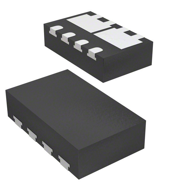
The Vishay Siliconix SI5999EDU-T1-GE3 is a dual P-channel MOSFET utilizing TrenchFET technology. It features a PowerPAK ChipFET Dual package with a maximum drain-source voltage of -20 V and a continuous drain current of -6 A at TC = 25 °C. The device exhibits a typical on-state resistance of 0.059 Ω at VGS = -4.5 V and 0.096 Ω at VGS = -2.5 V. Total gate charge is typically 6.9 nC at VGS = -4.5 V. Thermal resistance from junction to case is 9.5 °C/W, and the operating junction temperature range spans from -55 °C to +150 °C.
Verify component authenticity by cross-referencing the marking code OA XXX against official datasheet documentation. Confirm compliance with RoHS Directive 2002/95/EC and IEC 61249-2-21 halogen-free definitions during acquisition. Ensure sourcing channels provide valid traceability records and date codes matching the lot information printed on the package.
Select this component when a compact dual P-channel solution is required for low-voltage switching. The -20 V rating suits 3.3 V and 5 V logic systems. Evaluate thermal management requirements based on the 9.5 °C/W junction-to-case resistance. Verify that the PCB layout accommodates the specific PowerPAK ChipFET Dual pad dimensions outlined in application note 826.
This part belongs to the Vishay Siliconix Si5999EDU series of dual P-channel MOSFETs. It utilizes the PowerPAK ChipFET Dual package, which provides a thin 0.8 mm profile. The product is manufactured using TrenchFET technology to minimize on-resistance while maintaining a small footprint suitable for dense surface mount assemblies.
Direct replacement requires verifying pinout compatibility and electrical parameters. Check if alternative dual P-channel MOSFETs in similar packages meet the -20 V drain-source voltage and 0.059 Ω on-resistance specifications. Ensure the substitute package maintains the same thermal characteristics and physical dimensions.
 SI5999EDU-T1-GE3
The activity of extra discounts on wholesale prices is in full swing…
Please fill in your contact information and we will send you the latest wholesale price list.