ChipApex | Global Electronic Components Supplier
SEARCH
Search Product
Search Post
— IC芯片 | 连接器 | 传感器 | 被动器件 —
Search productSearch post
— IC芯片 | 连接器 | 传感器 | 被动器件 —
Consult the customer manager about the wholesale price.
consultation hotline:86-132-6715-2157
email:[email protected]
Contact the product manager for consultation. One-stop consultation is available.
Do you want a lower wholesale price? Please send us your inquiry and we will reply immediately.
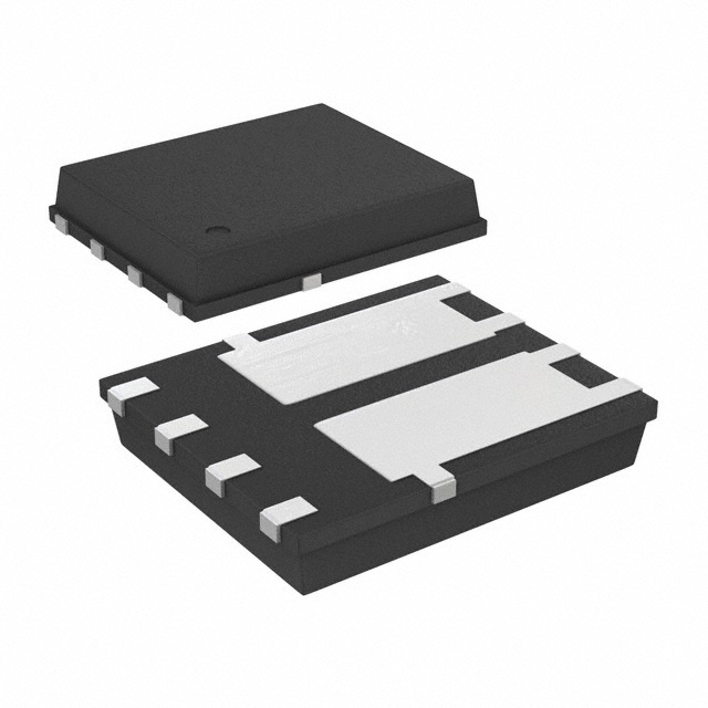
The SI7962DP-T1-E3 is a dual N-channel Power MOSFET manufactured by Vishay Siliconix, utilizing TrenchFET technology. It is housed in a compact PowerPAK SO-8 surface-mount package. The device features a drain-source voltage rating of 60 V and a continuous drain current of 14 A. Key electrical parameters include a maximum on-resistance of 15 mΩ at 10 V gate drive and a total gate charge of 22 nC. It supports an operating junction temperature range from -55°C to +150°C with a power dissipation capacity of 3.5 W.
Verify component authenticity through authorized distribution channels or direct manufacturer engagement. Confirm RoHS compliance status and specific lot traceability data prior to integration. Ensure storage conditions adhere to moisture sensitivity level requirements to maintain solderability and long-term reliability during PCB assembly processes.
Evaluate the 15 mΩ on-resistance against system efficiency targets at the intended operating current levels. Assess the 22 nC gate charge to determine driver capability requirements for optimal switching speeds. Compare the 3.5 W power dissipation limit with thermal design constraints to ensure adequate heat sinking or board layout provisions are implemented.
This component belongs to the Vishay SI79xxDP series of dual MOSFETs designed for high-efficiency power applications. It serves as a complementary counterpart to P-channel variants within the same package family, facilitating half-bridge and full-bridge topologies. The series emphasizes miniaturization without compromising current handling capabilities.
SI7962DN-T1-E3: Alternative pin-compatible variant with minor parameter differences.
The absolute maximum gate-source voltage rating is ±20 V.
Yes, the device is rated for a maximum junction temperature of +150°C.
The typical turn-on delay time is 10 ns under standard test conditions.
 SI7962DP-T1-E3
The activity of extra discounts on wholesale prices is in full swing…
Please fill in your contact information and we will send you the latest wholesale price list.