ChipApex | Global Electronic Components Supplier
SEARCH
Search Product
Search Post
— IC芯片 | 连接器 | 传感器 | 被动器件 —
Search productSearch post
— IC芯片 | 连接器 | 传感器 | 被动器件 —
Consult the customer manager about the wholesale price.
consultation hotline:86-132-6715-2157
email:[email protected]
Contact the product manager for consultation. One-stop consultation is available.
Do you want a lower wholesale price? Please send us your inquiry and we will reply immediately.
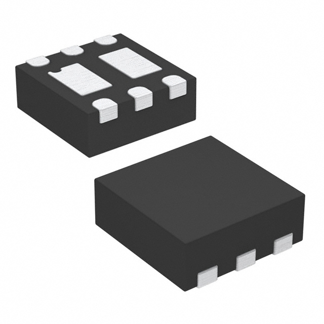
The SiA928DJ-T1-GE3 is a dual N-channel MOSFET from Vishay Siliconix, utilizing TrenchFET Gen IV technology. It features a thermally enhanced PowerPAK SC-70 package with dimensions of 2.05 mm by 2.05 mm. The device supports a drain-source voltage (VDS) of 30 V and a gate-source voltage (VGS) range of -16 V to +20 V. At VGS = 10 V, the maximum on-resistance (RDS(on)) is 0.025 Ω, while at VGS = 4.5 V, it is 0.033 Ω. The continuous drain current (ID) is rated at 4.5 A under case temperature conditions. Total gate charge (Qg) is typically 6.6 nC at VGS = 10 V.
Verify component authenticity through authorized distributors or direct manufacturer channels. Confirm datasheet revision status against the latest official documentation. Ensure ordering suffixes match specific packaging requirements such as reel quantities. Validate RoHS compliance documentation prior to procurement integration.
Evaluate thermal resistance ratings relative to the intended PCB layout and ambient operating conditions. Compare gate charge specifications against driver capabilities to ensure adequate switching speeds. Verify that the selected package dimensions align with the target board space constraints and soldering profile limitations.
This component belongs to the SiA series of power MOSFETs manufactured by Vishay Siliconix. It utilizes the PowerPAK SC-70 package family designed for high-density surface mount applications. The device integrates two independent N-channel MOSFETs into a single leadless package structure.
SiA928DJ-T1-GE3
The maximum junction-to-ambient thermal resistance is 65 °C/W.
The absolute maximum gate-source voltage limits are +20 V and -16 V.
The provided datasheet does not specify automotive qualification standards for this part number.
 SIA928DJ-T1-GE3
The activity of extra discounts on wholesale prices is in full swing…
Please fill in your contact information and we will send you the latest wholesale price list.