ChipApex | Global Electronic Components Supplier
SEARCH
Search Product
Search Post
— IC芯片 | 连接器 | 传感器 | 被动器件 —
Search productSearch post
— IC芯片 | 连接器 | 传感器 | 被动器件 —
Consult the customer manager about the wholesale price.
consultation hotline:86-132-6715-2157
email:[email protected]
Contact the product manager for consultation. One-stop consultation is available.
Do you want a lower wholesale price? Please send us your inquiry and we will reply immediately.
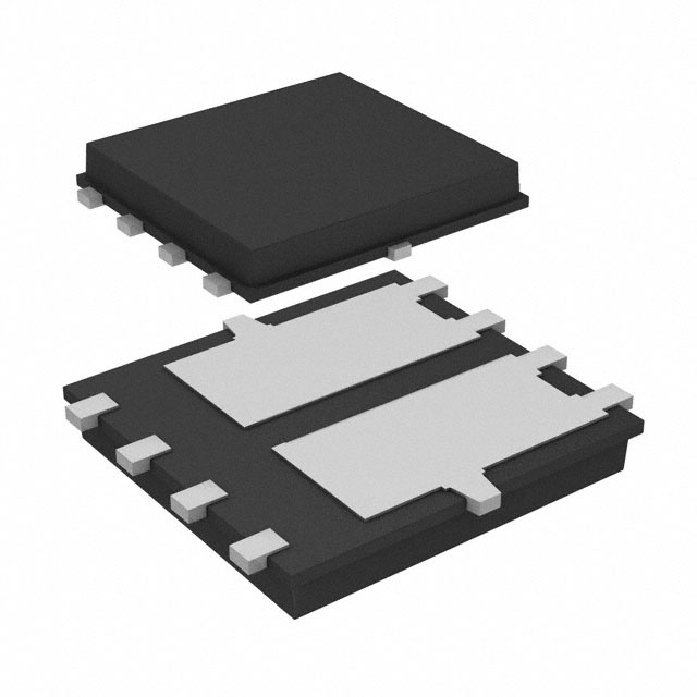
The SiS903DN is a dual P-channel MOSFET from Vishay Siliconix, utilizing TrenchFET Gen III technology. It features a PowerPAK 1212-8 package with dimensions of 3.3 mm x 3.3 mm. The device supports a drain-source voltage (VDS) of -20 V and offers low on-resistance values: 0.0201 Ω at VGS = -4.5 V, 0.0261 Ω at VGS = -2.5 V, and 0.0400 Ω at VGS = -1.8 V. Continuous drain current (ID) is rated at 6 A under steady-state conditions. Typical gate charge (Qg) is 15.9 nC at VGS = -2.5 V. Thermal resistance junction-to-case (RthJC) is typically 4.3 °C/W.
Verify the specific ordering suffix to confirm package type and compliance status. The SiS903DN-T1-GE3 designation indicates a lead-free and halogen-free product in the PowerPAK 1212-8 package. Confirm that the component meets material categorization requirements by referencing the official Vishay documentation for definitions of compliance before finalizing procurement specifications.
Select this component for applications requiring compact dual P-channel switching with low on-resistance. Ensure the gate drive voltage aligns with the specified thresholds for optimal RDS(on) performance. Verify thermal management capabilities against the junction-to-ambient and junction-to-case resistance ratings provided in the datasheet to maintain safe operating temperatures under expected load conditions.
This dual MOSFET integrates two independent P-channel switches into a single compact footprint. The PowerPAK 1212-8 package provides a smaller surface area compared to traditional SO-8 packages while maintaining robust thermal dissipation characteristics. The integration simplifies PCB layout for space-constrained designs requiring multiple switching functions.
No public confirmed substitute part numbers are documented in the source material.
 SIS903DN-T1-GE3
The activity of extra discounts on wholesale prices is in full swing…
Please fill in your contact information and we will send you the latest wholesale price list.