ChipApex | Global Electronic Components Supplier

SEARCH
Search Product
Search Post
— IC芯片 | 连接器 | 传感器 | 被动器件 —
Search productSearch post
— IC芯片 | 连接器 | 传感器 | 被动器件 —
Consult the customer manager about the wholesale price.
consultation hotline:86-132-6715-2157
email:[email protected]
Contact the product manager for consultation. One-stop consultation is available.
Do you want a lower wholesale price? Please send us your inquiry and we will reply immediately.
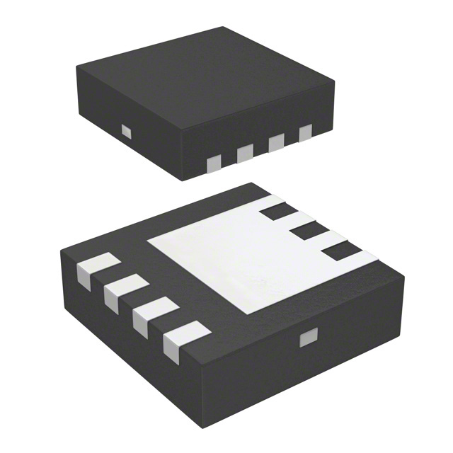
SISS61DN-T1-GE3 is listed in the Single FETs, MOSFETs range at ChipApex. The manufacturer field lists Vishay Siliconix. Its product description is MOSFET P-CH 20V 30.9/111.9A PPAK. Review the specifications below when checking this part for your BOM.
The Vishay Siliconix SISS61DN-T1-GE3 is a single P-channel MOSFET utilizing TrenchFET Gen III technology. It features a -20 V drain-source voltage rating and operates within a junction temperature range of -55 °C to +150 °C. The device is housed in a compact PowerPAK 1212-8S surface-mount package. Key electrical parameters include a maximum on-state resistance of 0.0035 Ω at VGS = -4.5 V, a typical total gate charge of 86 nC, and a continuous drain current capability of -111.9 A at TC = 25 °C.
Verify the specific ordering suffix against official documentation to confirm compliance attributes such as lead-free and halogen-free status. Ensure that the PowerPAK 1212-8S package dimensions align with the target PCB footprint. Confirm thermal management requirements based on the specified junction-to-case resistance values for the intended operating environment.
Select this component for designs requiring low on-resistance in a minimal footprint. Evaluate the gate charge specifications against driver capabilities to ensure adequate switching speeds. Consider the thermal derating curves when determining continuous current limits under varying case temperatures.
This part belongs to the Vishay Siliconix SiSS series of power MOSFETs. It utilizes the PowerPAK 1212-8S leadless package designed for high thermal efficiency. The device incorporates TrenchFET technology to optimize conduction losses while maintaining robust switching characteristics suitable for modern power management circuits.
Consult official substitution lists for verified alternatives. Cross-reference pinout configurations and absolute maximum ratings before integrating any substitute components into existing designs.
The absolute maximum gate-source voltage (VGS) is rated at ±8 V.
Yes, the datasheet specifies that 100% of the units are tested for unclamped inductive switching (UIS).
Explore related parts through FETs, MOSFETs, Transistors, Discrete Semiconductor Products, all product categories.
 SISS61DN-T1-GE3

The activity of extra discounts on wholesale prices is in full swing…
Please fill in your contact information and we will send you the latest wholesale price list.