ChipApex | Global Electronic Components Supplier
SEARCH
Search Product
Search Post
— IC芯片 | 连接器 | 传感器 | 被动器件 —
Search productSearch post
— IC芯片 | 连接器 | 传感器 | 被动器件 —
Consult the customer manager about the wholesale price.
consultation hotline:86-132-6715-2157
email:[email protected]
Contact the product manager for consultation. One-stop consultation is available.
Do you want a lower wholesale price? Please send us your inquiry and we will reply immediately.
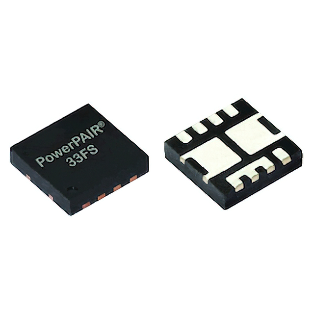
The SIZF5302DT-T1-RE3 is a dual N-channel 30 V (D-S) MOSFET from Vishay Siliconix, utilizing TrenchFET® Gen V technology. It features symmetric high-side and low-side configurations optimized for 50% duty cycles in flip-chip PowerPAIR® 3x3FS packages. Key electrical parameters include a maximum drain-source voltage of 30 V, continuous drain current of 100 A at TC = 25 °C, and typical gate charge of 6.7 nC at VGS = 4.5 V. The device offers a maximum on-state resistance of 3.2 mΩ at VGS = 10 V and 5.3 mΩ at VGS = 4.5 V.
Verify the specific ordering suffix against official documentation to confirm lead-free status and halogen-free compliance. Confirm package type matches the required PowerPAIR 3 x 3FS specifications. Ensure all technical parameters align with the application requirements before finalizing procurement decisions.
Select this component for designs requiring compact dual MOSFET solutions with high thermal performance. Evaluate the trade-off between on-resistance and gate charge based on switching frequency requirements. Consider the package's thermal characteristics when designing heat dissipation strategies for the target application environment.
This part belongs to the SiZF5300DT/SiZF5302DT series of 30 V symmetric dual N-channel MOSFETs. These devices are designed to replace two discrete PowerPAK 1212 components, offering significant space savings while maintaining high efficiency in power conversion applications.
Publicly confirmed substitute part numbers are not available in the provided documentation. Verify compatibility with existing designs by comparing absolute maximum ratings and thermal characteristics if considering alternative components.
The operating junction temperature range is -55 °C to +150 °C.
Yes, the device is 100% tested for both gate resistance (Rg) and unclamped inductive switching (UIS).
The typical total gate charge (Qg) at VDS = 15 V, VGS = 4.5 V, and ID = 20 A is 6.7 nC.
 SIZF5302DT-T1-RE3
The activity of extra discounts on wholesale prices is in full swing…
Please fill in your contact information and we will send you the latest wholesale price list.