 ChipApex | Global Electronic Components Supplier
SEARCH
Search Product
Search Post
— IC芯片 | 连接器 | 传感器 | 被动器件 —
Search productSearch post
— IC芯片 | 连接器 | 传感器 | 被动器件 —
Consult the customer manager about the wholesale price.
consultation hotline:86-132-6715-2157
email:[email protected]
Contact the product manager for consultation. One-stop consultation is available.
Do you want a lower wholesale price? Please send us your inquiry and we will reply immediately.
The SMMBFJ177LT1G is a P-Channel depletion mode JFET chopper manufactured by onsemi. It operates within a junction temperature range of -55°C to +150°C and features a maximum total device dissipation of 225 mW at 25°C ambient. The component provides a gate-source breakdown voltage of 30 Vdc, with a zero-gate-voltage drain current ranging from -1.5 mA to -20 mA at -15 Vds. Its maximum drain-source on resistance is 300 Ohms, and it exhibits an input capacitance of up to 11 pF at 1 MHz.
Verify the specific ordering suffix 'S' indicates AEC-Q101 qualification and PPAP capability requirements. Confirm package style matches the required pinout configuration for your PCB layout. Ensure compliance with RoHS directives if operating in restricted material zones. Validate thermal management strategies against the specified 225 mW dissipation limit.
Select this component when high-temperature stability and low leakage are critical. The P-Channel configuration suits negative rail or high-side switching applications. Verify that the 300 Ohm on-resistance meets the circuit's impedance requirements. Consider the SOT-23 footprint constraints during mechanical design integration.
This part belongs to the MMBFJ177 series of single P-Channel JFETs. It shares electrical characteristics with the standard MMBFJ177LT1G but includes the 'S' prefix for specialized automotive site controls. The device utilizes silicon technology housed in a compact SOT-23 surface-mount package.
Pin 1 is Drain, Pin 2 is Source, and Pin 3 is Gate.
Yes, the 'S' prefix denotes AEC-Q101 qualification and PPAP capability.
The maximum gate-source cutoff voltage is 2.5 Vdc.
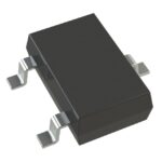 SMMBFJ177LT1G
The activity of extra discounts on wholesale prices is in full swing…
Please fill in your contact information and we will send you the latest wholesale price list.







