 ChipApex | Global Electronic Components Supplier
SEARCH
Search Product
Search Post
— IC芯片 | 连接器 | 传感器 | 被动器件 —
Search productSearch post
— IC芯片 | 连接器 | 传感器 | 被动器件 —
Consult the customer manager about the wholesale price.
consultation hotline:86-132-6715-2157
email:[email protected]
Contact the product manager for consultation. One-stop consultation is available.
Do you want a lower wholesale price? Please send us your inquiry and we will reply immediately.
The SN74SSTL16837ADGGR is a 20-bit universal bus driver designed for SSTL_3 interface applications. It operates with VCC and VDDQ supply voltages ranging from 3V to 3.6V, supporting SSTL_3 or LVTTL I/O levels. The device features a flow-through architecture and meets both SSTL_3 Class I and Class II specifications. It includes latch enable (LE) and clock (CLK) inputs for data storage, controlled by an output-enable (OE) input. The component is characterized for operation in the commercial temperature range of 0°C to 70°C.
Verify the specific suffix 'A' against the manufacturer's current documentation to confirm pinout and electrical parameter alignment with your design requirements. Ensure that the DGG package dimensions match your PCB footprint constraints. Confirm that the operating voltage range of 3V to 3.6V aligns with your system's VCC and VDDQ supplies before finalizing procurement.
Select this component when designing systems requiring a 20-bit wide data path with SSTL_3 compatibility. It is suitable for applications needing transparent mode operation or registered data storage via the LE and CLK pins. Consider the flow-through architecture if minimizing trace length and routing complexity on the PCB is a priority. Ensure the design supports the required VREF and VTT termination voltages for proper signal integrity.
This device belongs to Texas Instruments' Widebus family, which provides high-density logic solutions for complex digital systems. The SN74SSTL16837A variant specifically targets memory interface applications where SSTL_3 signaling is mandated. It serves as a bridge between processor buses and memory components, facilitating reliable data transmission at high frequencies up to 200 MHz.
Check for updated revisions within the SN74SSTL16837 series. Verify compatibility with other Widebus family members if system expansion is planned.
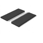 SN74SSTL16837ADGGR
The activity of extra discounts on wholesale prices is in full swing…
Please fill in your contact information and we will send you the latest wholesale price list.





