ChipApex | Global Electronic Components Supplier
SEARCH
Search Product
Search Post
— IC芯片 | 连接器 | 传感器 | 被动器件 —
Search productSearch post
— IC芯片 | 连接器 | 传感器 | 被动器件 —
Consult the customer manager about the wholesale price.
consultation hotline:86-132-6715-2157
email:[email protected]
Contact the product manager for consultation. One-stop consultation is available.
Do you want a lower wholesale price? Please send us your inquiry and we will reply immediately.
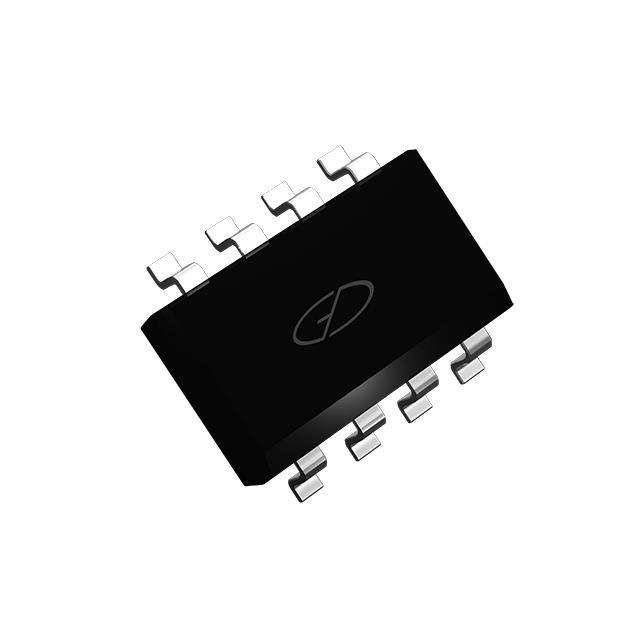
The SSFQ3812 is a dual N-channel MOSFET manufactured by Good-Ark Semiconductor, designed for high-efficiency switching applications. It features a drain-source voltage (Vdss) of 30 V and a continuous drain current (Id) of 7.5 A at 25°C case temperature. The device achieves a maximum on-resistance (Rds(on)) of 20 mΩ at Vgs=10V and 23 mΩ at Vgs=4.5V. Key electrical parameters include a gate threshold voltage (Vgs(th)) ranging from 1.2 V to 4.1 V, a total gate charge (Qg) of 15.8 nC at Vgs=10V, and an input capacitance (Ciss) of 345 pF. The component operates within a junction temperature range of -55°C to +150°C and utilizes an SOP-8 surface-mount package.
Verify the specific datasheet version against the manufacturer's official documentation before finalizing specifications. Confirm that the SOP-8 package dimensions and pinout align with the target PCB footprint requirements. Ensure thermal management strategies account for the specified junction-to-ambient thermal resistance values under actual operating conditions.
Select this component for designs requiring a compact dual-N channel solution with low conduction losses. The low gate charge facilitates faster switching speeds, reducing dynamic losses in high-frequency converters. Verify that the 30 V breakdown voltage provides sufficient margin for the intended circuit rail voltages and transient spikes.
This part belongs to the discrete semiconductor category, specifically within the single FET/MOSFET segment. It is classified as a metal-oxide semiconductor field-effect transistor utilizing enhancement mode operation. The device is intended for general-purpose switching applications where space constraints and power efficiency are critical design factors.
Consult official substitution lists or cross-reference databases for verified equivalent parts. Ensure any replacement maintains identical pin configurations, voltage ratings, and thermal characteristics to guarantee compatibility without redesigning the host circuit board.
The maximum continuous drain current is 7.5 A when measured at a case temperature of 25°C.
Yes, the datasheet specifies Drain-Source Diode Characteristics, indicating the presence of intrinsic body diodes associated with the MOSFET structure.
The on-resistance is specified at Vgs=10V and Vgs=4.5V, with lower resistance achieved at the higher voltage, suggesting 10V is preferred for minimal conduction loss.
 SSFQ3812
The activity of extra discounts on wholesale prices is in full swing…
Please fill in your contact information and we will send you the latest wholesale price list.