ChipApex | Global Electronic Components Supplier
SEARCH
Search Product
Search Post
— IC芯片 | 连接器 | 传感器 | 被动器件 —
Search productSearch post
— IC芯片 | 连接器 | 传感器 | 被动器件 —
Consult the customer manager about the wholesale price.
consultation hotline:86-132-6715-2157
email:[email protected]
Contact the product manager for consultation. One-stop consultation is available.
Do you want a lower wholesale price? Please send us your inquiry and we will reply immediately.
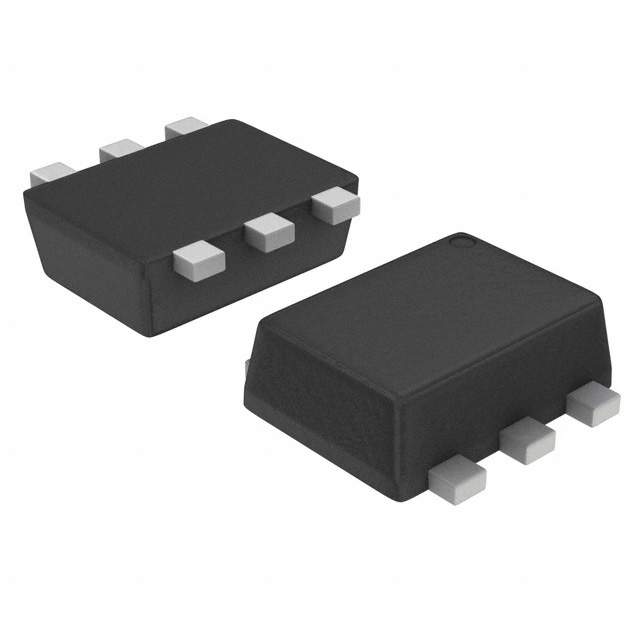
The SSM6L35FE,LM is a dual N-channel small signal MOSFET manufactured by Toshiba Semiconductor and Storage. It utilizes U-MOSIII technology within a UF-6 surface-mount package. The device features a drain-source breakdown voltage of 20 V. Continuous drain current ratings are specified at 0.1 A for the N-channel configuration. The maximum gate-source voltage is ±8 V. The component operates within a temperature range from -55 °C to +150 °C. Power dissipation is rated at 200 mW. The unit includes an internal diode structure.
Verify the exact suffix against official Toshiba documentation to confirm pinout and electrical tolerances. Ensure the ordering code matches the specific tape and reel requirements for automated assembly lines. Confirm RoHS compliance status through the manufacturer's latest release notes before finalizing procurement contracts.
Select this component for applications requiring low-voltage signal switching with minimal footprint constraints. The UF-6 package offers thermal efficiency suitable for dense PCB layouts. Verify that the 20 V rating exceeds the maximum circuit voltage under all transient conditions. Consider the 0.1 A current limit when designing load paths.
This part belongs to Toshiba's SSM6L series of dual MOSFETs designed for portable electronics. The series emphasizes low on-resistance and fast switching speeds. The UF-6 package is standard for space-constrained mobile devices. This specific variant integrates two N-channel devices for simplified circuit design.
Check Toshiba's official cross-reference list for verified equivalents. Ensure any substitute maintains the UF-6 footprint and 20 V rating. Verify compatibility with existing gate drive voltages and thermal management requirements.
 SSM6L35FE,LM
The activity of extra discounts on wholesale prices is in full swing…
Please fill in your contact information and we will send you the latest wholesale price list.