ChipApex | Global Electronic Components Supplier
SEARCH
Search Product
Search Post
— IC芯片 | 连接器 | 传感器 | 被动器件 —
Search productSearch post
— IC芯片 | 连接器 | 传感器 | 被动器件 —
Consult the customer manager about the wholesale price.
consultation hotline:86-132-6715-2157
email:[email protected]
Contact the product manager for consultation. One-stop consultation is available.
Do you want a lower wholesale price? Please send us your inquiry and we will reply immediately.
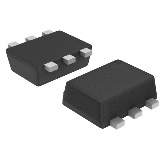
The SSM6N35AFE,LF is a dual N-channel silicon MOSFET in an ES6 (SOT-563) package. It supports 1.2 V drive with low on-resistance: max 9.0 Ω at VGS=1.2 V/ID=10 mA, and 1.1 Ω at VGS=4.5 V/ID=150 mA. Key ratings include VDSS of 20 V, continuous drain current ID of 250 mA, pulsed drain current IDP of 600 mA, and power dissipation PD of 150 mW. Gate-source voltage VGSS is ±10 V. Threshold voltage Vth ranges from 0.35 V to 1.0 V. Dynamic characteristics feature input capacitance Ciss of 18 pF typ., total gate charge Qg of 0.34 nC typ., turn-on delay td(on) of 2 ns typ., and fall time tf of 5.5 ns typ. Operating temperature spans -55 °C to +150 °C.
Verify the component against the official Toshiba datasheet specifications before integration. Confirm that the ES6 package dimensions and pin assignments match the design requirements. Ensure electrostatic discharge precautions are followed during handling. Check RoHS compliance status with the supplier if required by local regulations. Validate thermal performance under actual operating conditions.
Select this device for applications requiring dual N-channel MOSFETs with low-voltage drive capability. The 20 V breakdown voltage suits low-voltage signal paths. Consider the 150 mW power dissipation limit when designing heat dissipation strategies. The small ES6 package is suitable for space-constrained PCB layouts. Verify gate threshold voltage compatibility with the driving logic levels.
The SSM6N35AFE belongs to Toshiba's silicon N-channel MOSFET series. It is part of the commercial production lineup started in October 2016. The device is designed for general-purpose switching and analog applications. It utilizes standard silicon technology within a compact surface-mount form factor.
No public confirmed substitute part numbers are available in the provided documentation. Consult Toshiba representatives for potential alternatives.
The absolute maximum drain-source voltage (VDSS) is 20 V.
It contains two independent N-channel MOSFETs.
The typical total gate charge (Qg) is 0.34 nC at VDD=10 V, ID=200 mA, and VGS=4.5 V.
 SSM6N35AFE,LF
The activity of extra discounts on wholesale prices is in full swing…
Please fill in your contact information and we will send you the latest wholesale price list.