ChipApex | Global Electronic Components Supplier
SEARCH
Search Product
Search Post
— IC芯片 | 连接器 | 传感器 | 被动器件 —
Search productSearch post
— IC芯片 | 连接器 | 传感器 | 被动器件 —
Consult the customer manager about the wholesale price.
consultation hotline:86-132-6715-2157
email:[email protected]
Contact the product manager for consultation. One-stop consultation is available.
Do you want a lower wholesale price? Please send us your inquiry and we will reply immediately.
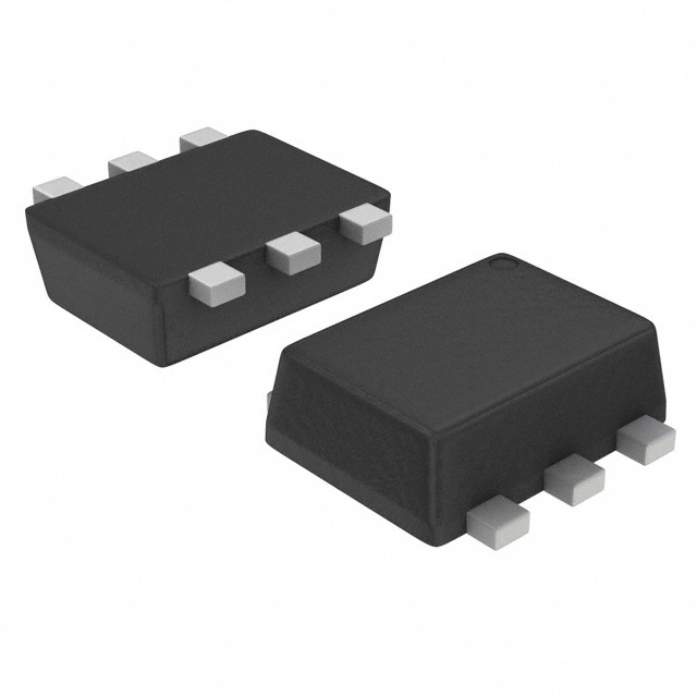
The SSM6N56FE,LM is a dual N-channel silicon MOSFET in an ES6 package. It supports high-speed switching with a drain-source voltage of 20 V and continuous current of 800 mA. The device features low on-resistance: 235 mΩ at VGS=4.5V/ID=800mA, 300 mΩ at VGS=2.5V/ID=600mA, 480 mΩ at VGS=1.8V/ID=200mA, and 840 mΩ at VGS=1.5V/ID=50mA. Gate threshold voltage ranges from 0.4 V to 1.0 V. Switching times are 5.5 ns (ton) and 8.5 ns (toff). Total gate charge is typically 1.0 nC. Power dissipation is 150 mW or 250 mW depending on board conditions. Operating temperature spans -55°C to +150°C.
Verify the component against the official Toshiba datasheet revision Rev.1.0.A dated 2014-04-10. Confirm the ES6 package marking and pin assignment matches the source documentation. Ensure design compliance with absolute maximum ratings, particularly regarding channel temperature limits and electrostatic discharge precautions during handling.
Select this component when low on-resistance is required at reduced gate voltages such as 1.5 V or 1.8 V. The dual configuration allows space-efficient designs. Consider thermal dissipation capabilities based on the specific PCB copper pad area, as power ratings vary between 150 mW and 250 mW depending on the mounting conditions.
This part belongs to the SSM6N56 series of small-signal MOSFETs manufactured by Toshiba Semiconductor and Storage. It utilizes U-MOSVII-H technology. The ES6 package provides a compact footprint suitable for surface-mount assembly. The device integrates two independent N-channel MOSFETs within a single housing.
Consult the manufacturer's cross-reference data for verified substitutes. No public substitute part numbers are confirmed in the provided documentation.
 SSM6N56FE,LM
The activity of extra discounts on wholesale prices is in full swing…
Please fill in your contact information and we will send you the latest wholesale price list.