 ChipApex | Global Electronic Components Supplier
SEARCH
Search Product
Search Post
— IC芯片 | 连接器 | 传感器 | 被动器件 —
Search productSearch post
— IC芯片 | 连接器 | 传感器 | 被动器件 —
Consult the customer manager about the wholesale price.
consultation hotline:86-132-6715-2157
email:[email protected]
Contact the product manager for consultation. One-stop consultation is available.
Do you want a lower wholesale price? Please send us your inquiry and we will reply immediately.
The SSM6P36TU,LF is a dual P-channel silicon MOSFET in the UF-6 (SOT-363F) surface-mount package. It features a drain-source voltage of -20 V and a continuous drain current of -330 mA. The device supports low-voltage drive with an ON-resistance of 1.31 Ω max at VGS = -4.5 V, 1.60 Ω max at -2.8 V, 2.70 Ω max at -1.8 V, and 3.60 Ω max at -1.5 V. Total gate charge is typically 1.2 nC. Power dissipation reaches 500 mW on an FR4 board, with an operating temperature range from -55 °C to +150 °C.
Verify component authenticity by matching the manufacturer marking code 'T 2-2T1B' against official datasheet specifications. Confirm the ordering suffix ',LF' indicates lead-free compliance. Ensure the UF-6 package dimensions align with PCB footprint requirements before finalizing procurement orders.
Select this component when designing circuits requiring dual P-channel isolation within a minimal footprint. Verify that the required gate drive voltage meets the threshold characteristics for the desired ON-resistance level. Ensure thermal design accommodates the 500 mW dissipation limit under expected load conditions.
This part belongs to Toshiba's small-signal MOSFET portfolio designed for portable electronics. It utilizes U-MOSIII technology to achieve high switching speeds and low ON-resistance within the compact UF-6 package, serving as a space-efficient alternative to discrete single-channel solutions.
Direct pin-compatible replacements include the SSM6N36TU,LF for N-channel applications or other SSM6 series variants with matching UF-6 footprints. Verify electrical parameters such as RDS(ON) and VDSS match circuit requirements before substitution.
The absolute maximum gate-source voltage (VGSS) rating is ±8 V.
RDS(ON) decreases as the magnitude of the negative gate-source voltage increases, ranging from 3.60 Ω max at -1.5 V to 1.31 Ω max at -4.5 V.
The typical turn-off time (toff) is 200 ns under test conditions of VDD = -10 V, ID = -100 mA, and RG = 50 Ω.
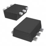 SSM6P36TU,LF
The activity of extra discounts on wholesale prices is in full swing…
Please fill in your contact information and we will send you the latest wholesale price list.





