ChipApex | Global Electronic Components Supplier
SEARCH
Search Product
Search Post
— IC芯片 | 连接器 | 传感器 | 被动器件 —
Search productSearch post
— IC芯片 | 连接器 | 传感器 | 被动器件 —
Consult the customer manager about the wholesale price.
consultation hotline:86-132-6715-2157
email:[email protected]
Contact the product manager for consultation. One-stop consultation is available.
Do you want a lower wholesale price? Please send us your inquiry and we will reply immediately.
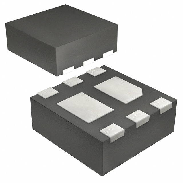
The SSM6P49NU,LF is a dual P-channel MOSFET manufactured by Toshiba Semiconductor and Storage. It utilizes U-MOSVI technology in a UDFN-6 surface-mount package. The device features a drain-source breakdown voltage of 20 V and a continuous drain current of -4 A. Its typical on-resistance is 157 mOhms with a gate-source voltage range of ±12 V. The threshold voltage is specified at 1.2 V. Operating temperatures range from -55°C to +150°C, with a power dissipation rating of 1 W.
Verify the complete part number including the LF suffix to confirm lead-free compliance status. Confirm the specific manufacturing date code against project requirements. Ensure the UDFN-6 footprint matches the PCB layout specifications. Validate thermal resistance parameters for the intended enclosure environment. Cross-reference the datasheet revision to ensure compatibility with existing design documentation.
Select this component when a dual P-channel configuration is required within a UDFN-6 footprint. The 20 V rating suits low-voltage systems. The 157 mOhm on-resistance balances conduction losses with switching speed. Consider the 1 W power dissipation limit for thermal management planning. Verify that the 12 V gate drive capability aligns with the system logic levels.
This component belongs to the SSM6P49 series of dual MOSFETs from Toshiba. It shares the UDFN-6 package form factor with other small-signal devices in the lineup but differs in channel count and current ratings compared to single-channel variants like the SSM6J501NU. The U-MOSVI process node distinguishes it from older generations using different technology names.
Direct substitutes must match the dual P-channel topology, 20 V rating, and UDFN-6 package. Verify pinout compatibility before substitution. Check if alternative manufacturers offer equivalent Rds(on) and current capabilities within the same thermal constraints.
 SSM6P49NU,LF
The activity of extra discounts on wholesale prices is in full swing…
Please fill in your contact information and we will send you the latest wholesale price list.