ChipApex | Global Electronic Components Supplier

SEARCH
Search Product
Search Post
— IC芯片 | 连接器 | 传感器 | 被动器件 —
Search productSearch post
— IC芯片 | 连接器 | 传感器 | 被动器件 —
Consult the customer manager about the wholesale price.
consultation hotline:86-132-6715-2157
email:[email protected]
Contact the product manager for consultation. One-stop consultation is available.
Do you want a lower wholesale price? Please send us your inquiry and we will reply immediately.
THS4502IDGN is listed in the Instrumentation, Op Amps, Buffer Amps range at ChipApex. The manufacturer field lists Texas Instruments. Its product description is IC OPAMP DIFF 1 CIRCUIT 8HVSSOP. Review the specifications below when checking this part for your BOM.
The THS4502IDGN is a high-speed fully differential amplifier from Texas Instruments, housed in an 8-pin MSOP PowerPAD package. It features a bandwidth of 370 MHz and a slew rate of 2800 V/µs. The device supports a wide supply voltage range including ±5 V, ±12 V, and 15 V single-ended operation. Key electrical characteristics include a common-mode rejection ratio (CMRR) of 80 dB and a third-order intermodulation distortion (IMD3) of -95 dBc at 30 MHz. It includes power-down capability with a quiescent current of 1 mA in the disabled state.
Verify the specific suffix IDGN corresponds to the industrial temperature range (-40°C to +85°C) and the MSOP PowerPAD package configuration. Confirm that the ordering part number matches the required tape-and-reel or tube packaging quantity specified by the manufacturer. Ensure thermal management design accounts for the PowerPAD heatsink requirement to prevent oscillation above 60°C junction temperature.
Select this component for applications requiring high-speed signal conversion with low distortion. Compare against the THS4503 if power-down functionality is not needed. Consider the THS4501 for designs requiring rail-to-rail input/output capabilities. Evaluate thermal dissipation requirements carefully due to the sensitivity of the device to die temperatures exceeding 60°C.
The THS4502 belongs to the THS450x family of wideband, low-distortion fully differential amplifiers. It shares performance metrics with the THS4503 but adds power-down control via the PD pin. This family is designed to drive high-speed ADCs and support wireless infrastructure applications where signal integrity and dynamic range are critical.
THS4503IDGN is the direct functional substitute without power-down capability. THS4501IDGN offers similar speed but with rail-to-rail I/O. Verify pin compatibility and thermal characteristics before substitution.
The device may exhibit low-level oscillation if the die temperature exceeds +60°C. Designers must ensure adequate thermal management to keep the junction temperature below this threshold.
In the power-down state, the input impedance changes to approximately 50 Ω || 1 kΩ || pF, differing from the typical 10^7 Ω || 1 Ω || pF in normal operation.
Explore related parts through Amplifiers, Linear, Integrated Circuits (ICs), all product categories.
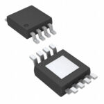 THS4502IDGN

The activity of extra discounts on wholesale prices is in full swing…
Please fill in your contact information and we will send you the latest wholesale price list.