 ChipApex | Global Electronic Components Supplier

SEARCH
Search Product
Search Post
— IC芯片 | 连接器 | 传感器 | 被动器件 —
Search productSearch post
— IC芯片 | 连接器 | 传感器 | 被动器件 —
Consult the customer manager about the wholesale price.
consultation hotline:86-132-6715-2157
email:[email protected]
Contact the product manager for consultation. One-stop consultation is available.
Do you want a lower wholesale price? Please send us your inquiry and we will reply immediately.
TMUX646ZECR is listed in the Analog Switches - Special Purpose range at ChipApex. The manufacturer field lists Texas Instruments. Its product description is IC MULTIPLEXER. Review the specifications below when checking this part for your BOM.
The TMUX646ZECR is a 10-channel (5 differential) single-pole, double-throw bidirectional analog switch manufactured by Texas Instruments. It operates within a supply voltage range of 1.5 V to 5.5 V and supports logic inputs compatible with 1.2 V and 1.8 V standards. The device provides a bandwidth of 6 GHz with a typical on-resistance of 6 Ω and ultra-low crosstalk of -40 dB at 1250 MHz. It features powered-off protection, maintaining high impedance when VDD is 0 V. The component is housed in a 36-pin nFBGA package (ZEC) measuring 2.45 mm × 2.45 mm.
Verify the specific ordering suffix ZECR corresponds to the nFBGA-36 package and reel packaging configuration before procurement. Confirm that the 1.5 V to 5.5 V supply range aligns with the target system design requirements. Ensure compliance with RoHS directives as indicated in the manufacturer specifications. Check for any moisture sensitivity level requirements during storage and handling procedures.
Select this component for applications requiring high-speed signal switching between multiple MIPI modules and a single processor port. The 6 GHz bandwidth and low skew characteristics make it suitable for demanding video and data interfaces. Consider the 1.2 V logic compatibility if interfacing with lower voltage processors without external translators. Evaluate the thermal resistance metrics for adequate heat dissipation in dense layouts.
The TMUX646 belongs to the TMUX646 series of optimized high-speed switches designed for MIPI compliant devices. It facilitates connecting multiple MIPI modules to a single CSI/DSI or C-PHY/D-PHY module. The device expands system capabilities by allowing a single MIPI port to interface with two distinct MIPI modules, addressing port limitations in compact electronics.
Consult the official datasheet orderable addendum for available package variations and potential cross-references. Verify functional equivalence regarding pinout, electrical characteristics, and package dimensions before substitution.
When VDD is 0 V, the I/Os and digital logic pins remain in a high-impedance state, preventing back-powering and maintaining isolation.
The SEL and OE pins support 1.2 V logic compatible inputs, eliminating the need for external voltage translators regardless of the VDD voltage.
Yes, the clock and data lanes can be interchanged to facilitate optimal layout for D-PHY and C-PHY applications.
Explore related parts through Interface, Integrated Circuits (ICs), all product categories, ChipApex homepage.
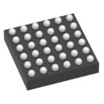 TMUX646ZECR

The activity of extra discounts on wholesale prices is in full swing…
Please fill in your contact information and we will send you the latest wholesale price list.





