 ChipApex | Global Electronic Components Supplier

SEARCH
Search Product
Search Post
— IC芯片 | 连接器 | 传感器 | 被动器件 —
Search productSearch post
— IC芯片 | 连接器 | 传感器 | 被动器件 —
Consult the customer manager about the wholesale price.
consultation hotline:86-132-6715-2157
email:[email protected]
Contact the product manager for consultation. One-stop consultation is available.
Do you want a lower wholesale price? Please send us your inquiry and we will reply immediately.
TN5335N8-G is listed in the Single FETs, MOSFETs range at ChipApex. The manufacturer field lists Microchip Technology. Its product description is MOSFET N-CH 350V 230MA TO243AA. Review the specifications below when checking this part for your BOM.
The TN5335N8-G is an N-Channel Enhancement-Mode Vertical DMOS FET manufactured by Microchip Technology. It utilizes a silicon-gate process and features a 3-lead SOT-89 package. Key electrical specifications include a drain-to-source breakdown voltage of 350 V, a maximum static on-state resistance of 15 Ω, and a gate threshold voltage of 2 V. The device supports a continuous drain current of 230 mA and dissipates up to 1.6 W at 25°C ambient temperature. Operating temperatures range from -55°C to +150°C.
Verify the specific suffix 'N8' corresponds to the 3-lead SOT-89 package configuration during procurement. Confirm RoHS compliance status as indicated by the '-G' designation. Ensure the ordering quantity matches the standard reel packaging specification of 2000 units per reel. Cross-reference the datasheet revision DS20005955A for accurate pinout details before integration.
Select this component when high breakdown voltage and low on-resistance are required in a compact surface-mount form factor. The SOT-89 package offers higher power dissipation capabilities compared to smaller alternatives like SOT-23. Consider the 15 Ω on-state resistance and 230 mA continuous current limits for load requirements. Verify that the application operates within the specified -55°C to +150°C temperature range.
The TN5335 series comprises N-Channel and P-Channel Enhancement-Mode Vertical DMOS FETs. The TN5335N8-G specifically denotes the N-Channel variant housed in a 3-lead SOT-89 package. This family is designed for switching and amplifying applications requiring fast switching speeds and low input capacitance. The device combines bipolar-like power handling with MOSFET characteristics.
The TN5335K1-G serves as a direct functional substitute within the same series, differing only in package type (SOT-23 instead of SOT-89). Designers must account for differences in thermal resistance and physical footprint when substituting between these package variants.
The absolute maximum rating for gate-to-source voltage is ±20V.
No, the device is free from thermal runaway due to its positive temperature coefficient inherent in MOS structures.
Explore related parts through FETs, MOSFETs, Transistors, Discrete Semiconductor Products, all product categories.
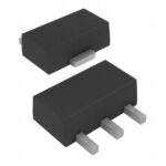 TN5335N8-G

The activity of extra discounts on wholesale prices is in full swing…
Please fill in your contact information and we will send you the latest wholesale price list.





