ChipApex | Global Electronic Components Supplier
SEARCH
Search Product
Search Post
— IC芯片 | 连接器 | 传感器 | 被动器件 —
Search productSearch post
— IC芯片 | 连接器 | 传感器 | 被动器件 —
Consult the customer manager about the wholesale price.
consultation hotline:86-132-6715-2157
email:[email protected]
Contact the product manager for consultation. One-stop consultation is available.
Do you want a lower wholesale price? Please send us your inquiry and we will reply immediately.
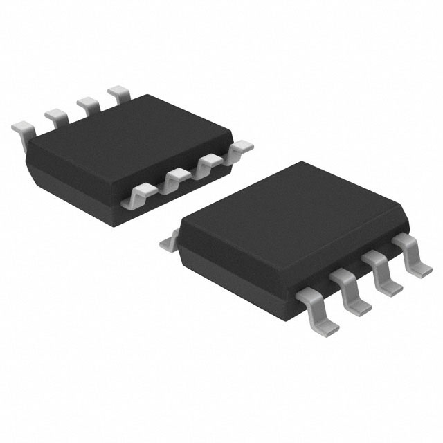
The TPC8212-H is a silicon N-channel MOS field-effect transistor utilizing Ultra-High-Speed U-MOSIII technology. It features a drain-source voltage of 30 V and a continuous drain current of 6 A. The device exhibits a typical drain-source ON-resistance of 16 mΩ at VGS = 10 V and ID = 3 A, with a forward transfer admittance of 14 S. Gate charge is typically 5.5 nC. Thermal resistance from channel to ambient is 83.3 °C/W for single-device operation on glass-epoxy board (a).
Verify the specific ordering suffix TE12LQ against official Toshiba documentation to confirm tape-and-reel packaging specifications. Ensure compliance with RoHS directives by checking the most recent product specifications or contacting the manufacturer directly, as environmental data may vary by production batch.
Select this component for designs requiring low ON-resistance and fast switching speeds within a 30 V limit. Consider the thermal resistance values when designing heat dissipation strategies, particularly for dual-operation configurations where power is evenly distributed between devices.
This part belongs to Toshiba's U-MOSIII family of ultra-high-speed MOSFETs. It is designed specifically for portable electronics and notebook PCs where space constraints and switching efficiency are critical. The device integrates advanced trench gate technology to minimize conduction losses while maintaining robust avalanche capabilities.
Publicly confirmed substitute part numbers are not available in the provided source material. Consult Toshiba's cross-reference tools or distributor databases for parametrically similar alternatives if direct replacement is required.
The maximum drain-source breakdown voltage (V(BR)DSS) is 30 V when measured at ID = 10 mA and VGS = 0 V.
The gate threshold voltage (Vth) ranges from 1.1 V to 2.3 V at Ta = 25°C. Graphical data indicates that Vth decreases as ambient temperature increases.
The typical total gate charge (Qg) is 16 nC under conditions of VDD = -24 V, VGS = 10 V, and ID = 6 A.
 TPC8212-H(TE12LQ,M
The activity of extra discounts on wholesale prices is in full swing…
Please fill in your contact information and we will send you the latest wholesale price list.