ChipApex | Global Electronic Components Supplier
SEARCH
Search Product
Search Post
— IC芯片 | 连接器 | 传感器 | 被动器件 —
Search productSearch post
— IC芯片 | 连接器 | 传感器 | 被动器件 —
Consult the customer manager about the wholesale price.
consultation hotline:86-132-6715-2157
email:[email protected]
Contact the product manager for consultation. One-stop consultation is available.
Do you want a lower wholesale price? Please send us your inquiry and we will reply immediately.
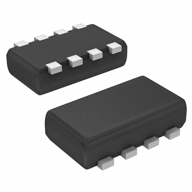
The TT8J2TR is a dual P-channel MOSFET manufactured by ROHM Semiconductor, designed for low-voltage drive applications. It features a TSST8 surface-mount package with eight terminals. Key electrical parameters include a drain-source voltage (V_DSS) of -30 V and a continuous drain current (I_D) of ±2.5 A. The device exhibits low on-state resistance, typically 115 mΩ at V_GS = -4 V and 60 mΩ at V_GS = -10 V. Total gate charge (Q_g) is 4.8 nC, supporting fast switching capabilities. Power dissipation is rated at 1.25 W total, with a maximum junction temperature of 150°C.
Verify the specific ordering suffix against official documentation to confirm packaging details. Confirm RoHS compliance status through the manufacturer's latest release notes. Ensure that ESD protection measures are integrated into the circuit design as recommended in the product notice section of the datasheet.
Select this component for applications requiring dual P-channel configuration in a compact surface-mount footprint. Evaluate the thermal resistance characteristics relative to the intended PCB layout. Consider the gate threshold voltage range when designing the driving circuitry to ensure reliable turn-on and turn-off states under varying load conditions.
This part belongs to the ROHM discrete semiconductor product line, specifically within the FET and MOSFET array category. It utilizes silicon technology and is housed in an 8-terminal TSST8 package. The device is engineered for general-use electronic devices, providing a balance between switching speed and conduction loss in small form-factor designs.
No public confirmed substitute part numbers are available in the provided documentation. Verify pinout compatibility and electrical ratings if considering alternative manufacturers for redesign purposes.
The typical static drain-source on-state resistance (R_DS(on)) is 115 mΩ when measured at a drain current of -1.2 A and a gate-source voltage of -4 V.
Yes, the inner circuit diagram indicates the presence of body diodes connected between the source and drain of each channel.
The absolute maximum rating for the gate-source voltage (V_GSS) is ±20 V.
 TT8J2TR
The activity of extra discounts on wholesale prices is in full swing…
Please fill in your contact information and we will send you the latest wholesale price list.