ChipApex | Global Electronic Components Supplier
SEARCH
Search Product
Search Post
— IC芯片 | 连接器 | 传感器 | 被动器件 —
Search productSearch post
— IC芯片 | 连接器 | 传感器 | 被动器件 —
Consult the customer manager about the wholesale price.
consultation hotline:86-132-6715-2157
email:[email protected]
Contact the product manager for consultation. One-stop consultation is available.
Do you want a lower wholesale price? Please send us your inquiry and we will reply immediately.
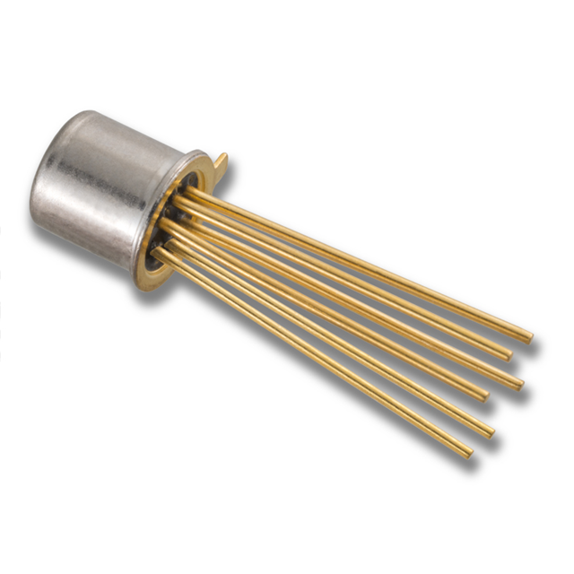
The U402 is a monolithic dual N-channel JFET switch manufactured by Linear Integrated Systems. It integrates two independent JFET elements within a single silicon die, housed in a TO-71 cylindrical metal package with six wire leads. The device is engineered for low noise and minimal parameter drift over temperature variations. Key electrical characteristics include a typical pinch-off voltage of 2.5V and a gate-source voltage drift of 10µV/°C. The input noise density is specified at 6nV/√Hz at 10Hz. It operates as an enhancement mode device suitable for precision analog switching applications.
Verify the manufacturer origin carefully, as multiple entities including Calogic and Micross Components have produced variants of this part number. Confirm the specific package style matches the required TO-71 form factor. Check for RoHS compliance status as historical production runs may differ from current stock. Ensure the pinout configuration aligns with the intended circuit design before finalizing procurement orders.
Select this component when application requirements demand extremely low offset voltage drift and minimal input noise in a dual-switch configuration. The TO-71 package is suitable for through-hole mounting where space constraints allow for larger footprints compared to surface-mount alternatives. Consider the specific pinch-off voltage tolerance if precise control over the off-state resistance is critical for the system design.
This component belongs to a family of low-noise, low-drift monolithic JFET switches originally developed by Siliconix and later acquired or continued by Linear Integrated Systems and other manufacturers. The U402 specifically denotes the dual N-channel variant packaged in the standard TO-71 metal can. It serves as a direct replacement for legacy discrete JFET pairs that previously occupied significant board space and exhibited higher parameter mismatches.
The typical input noise density is 6nV/√Hz measured at a frequency of 10Hz.
The U402 contains two separate N-channel JFET elements integrated on a single monolithic die.
The typical gate-source voltage drift is 10µV/°C, indicating high thermal stability.
 U402 TO-71 6L ROHS
The activity of extra discounts on wholesale prices is in full swing…
Please fill in your contact information and we will send you the latest wholesale price list.