 ChipApex | Global Electronic Components Supplier
SEARCH
Search Product
Search Post
— IC芯片 | 连接器 | 传感器 | 被动器件 —
Search productSearch post
— IC芯片 | 连接器 | 传感器 | 被动器件 —
Consult the customer manager about the wholesale price.
consultation hotline:86-132-6715-2157
email:[email protected]
Contact the product manager for consultation. One-stop consultation is available.
Do you want a lower wholesale price? Please send us your inquiry and we will reply immediately.
The VEC2315-TL-W is a dual P-channel power MOSFET manufactured by onsemi using trench technology. It operates with a drain-to-source voltage of -60V and a continuous drain current of -2.5A. The device features low on-resistance, specified at 137mΩ maximum at -10V gate drive and 180mΩ at -4.5V. Packaged in an SOT-28FL (VEC8) format, it includes ESD diode protection for the gate. Key electrical parameters include a total gate charge of 11nC and a junction temperature rating up to 150°C.
Verify the specific ordering suffix 'W' against official documentation to confirm tape and reel specifications. Confirm that the component meets Pb-Free, Halogen Free, and RoHS compliance requirements as stated in the datasheet. Ensure the selected packaging aligns with the required quantity per reel for the manufacturing process.
Select this component when a dual P-channel solution is required within a compact footprint. The device is suitable for designs needing logic-level compatibility at -4.5V or standard -10V drive levels. Evaluate thermal resistance ratings based on the specific PCB copper area available for heat dissipation during operation.
This part belongs to the VEC2315 family of power MOSFETs produced by onsemi. The product utilizes advanced trench technology to achieve optimized switching characteristics and conduction losses. It is distinct from other variants in the series primarily through its specific packaging and marking configuration.
Direct replacements must match the -60V rating, dual P-channel topology, and VEC8 package dimensions. Verify that alternative components offer comparable RDS(on) values at the intended gate drive voltages to maintain circuit efficiency.
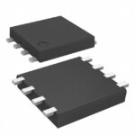 VEC2315-TL-W
The activity of extra discounts on wholesale prices is in full swing…
Please fill in your contact information and we will send you the latest wholesale price list.





