ChipApex | Global Electronic Components Supplier
SEARCH
Search Product
Search Post
— IC芯片 | 连接器 | 传感器 | 被动器件 —
Search productSearch post
— IC芯片 | 连接器 | 传感器 | 被动器件 —
Consult the customer manager about the wholesale price.
consultation hotline:86-132-6715-2157
email:[email protected]
Contact the product manager for consultation. One-stop consultation is available.
Do you want a lower wholesale price? Please send us your inquiry and we will reply immediately.
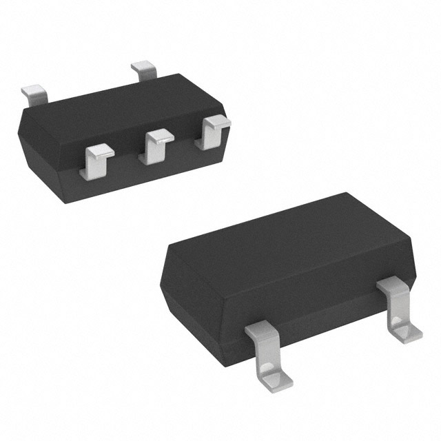
The XN01872 is a silicon n-channel enhancement MOSFET composite transistor designed for switching applications. It integrates two source-coupled FETs into a single EIAJ SC-74A Mini5-G1 package, effectively halving the required mounting area and assembly costs compared to discrete components. The device features a drain-source voltage rating of 50 V and a continuous drain current of 100 mA. Key electrical characteristics include a gate threshold voltage ranging from 1.5 V to 3.5 V and a typical forward transfer admittance of 30 mS at 25°C. The component operates within an ambient temperature range of -55°C to +150°C storage and up to 125°C operation, with a channel temperature limit of 150°C.
Verify the specific lifecycle status before procurement, as the datasheet indicates this product falls under maintenance or discontinued categories. Confirm that the final specifications align with current requirements, as Panasonic reserves the right to modify product standards without notice. Ensure compliance with export control laws if transferring technical data across borders.
Select this component when space constraints require integrating multiple switching elements into a single footprint. The 50V rating and 100mA current capacity suit low-voltage logic interfaces. Verify that the 1.5V to 3.5V gate threshold voltage matches the driving logic levels of the target application to ensure reliable turn-on and turn-off performance.
This part corresponds to the conventional designation 2SK0621 (or 2SK621). It represents a dual-element configuration where two identical n-channel enhancement mode MOSFETs are packaged together. This integration simplifies circuit design by reducing the number of individual components needed for parallel or complementary switching tasks.
The datasheet explicitly identifies the conventional part number 2SK0621 (2SK621) as the equivalent designation. No other substitute part numbers are documented in the provided source material.
The device incorporates two separate n-channel enhancement MOSFETs within a single package. Pin 1 and Pin 2 serve as the drains for FET1 and FET2 respectively, while Pin 4 acts as the common source.
The maximum gate-source voltage (VGSO) with the drain open is rated at 8 V. Exceeding this limit may damage the device.
By incorporating two elements into one package, the component reduces the required mounting area on the printed circuit board and halves the assembly costs associated with placing individual discrete transistors.
 XN0187200L
The activity of extra discounts on wholesale prices is in full swing…
Please fill in your contact information and we will send you the latest wholesale price list.