 ChipApex | Global Electronic Components Supplier
SEARCH
Search Product
Search Post
— IC芯片 | 连接器 | 传感器 | 被动器件 —
Search productSearch post
— IC芯片 | 连接器 | 传感器 | 被动器件 —
Consult the customer manager about the wholesale price.
consultation hotline:86-132-6715-2157
email:[email protected]
Contact the product manager for consultation. One-stop consultation is available.
Do you want a lower wholesale price? Please send us your inquiry and we will reply immediately.
The ZXMC3A16DN8TA is a complementary enhancement mode MOSFET array manufactured by Diodes Incorporated, housed in an SO-8 surface-mount package. The N-channel device features a drain-source voltage of 30V and a maximum continuous drain current of 6.4A at 25°C, with a typical on-resistance of 0.035 ohms. The P-channel counterpart provides a -30V rating and a -5.4A continuous drain current, exhibiting a typical on-resistance of 0.048 ohms. Both channels are designed for low threshold operation and fast switching speeds.
Verify the component against the official datasheet specifications to ensure compatibility with the intended circuit design. Confirm that the SO-8 package dimensions and pinout align with the PCB footprint requirements. Ensure thermal management strategies account for the specified power dissipation ratings under actual operating conditions.
Select this component for applications requiring high-efficiency, low-voltage power management where fast switching is critical. Consider the specific on-resistance values at different gate voltages when designing the drive circuitry. Evaluate the thermal resistance parameters relative to the PCB copper area to ensure reliable operation within the specified temperature range.
This part belongs to the Zetex generation of trench MOSFETs from Diodes Incorporated. It is marketed as a new generation solution combining low on-resistance with fast switching capabilities. The device is specifically engineered for high efficiency in low voltage power management applications.
No official substitutes are listed in the documentation. When evaluating alternatives, verify that the replacement maintains the same SO-8 package outline and pin configuration. Ensure the substitute components meet or exceed the 30V breakdown voltage and current handling capabilities required by the original design.
The operating and storage temperature range extends up to +150°C.
Thermal resistance varies based on PCB copper coverage; it ranges from 60°C/W to 100°C/W depending on whether one or both dies are active and the extent of copper coverage.
The typical input capacitance is 796 pF, measured at VDS=25V, VGS=0V, and f=1MHz.
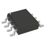 ZXMC3A16DN8TA
The activity of extra discounts on wholesale prices is in full swing…
Please fill in your contact information and we will send you the latest wholesale price list.





