 ChipApex | Global Electronic Components Supplier
SEARCH
Search Product
Search Post
— IC芯片 | 连接器 | 传感器 | 被动器件 —
Search productSearch post
— IC芯片 | 连接器 | 传感器 | 被动器件 —
Consult the customer manager about the wholesale price.
consultation hotline:86-132-6715-2157
email:[email protected]
Contact the product manager for consultation. One-stop consultation is available.
Do you want a lower wholesale price? Please send us your inquiry and we will reply immediately.
The ZXMD63N03XTA is a dual N-channel enhancement mode MOSFET manufactured by Diodes Incorporated. It features a maximum drain-source voltage of 30V and a continuous drain current of 2.3A at +25°C. The device offers a low on-state resistance of 135mΩ at VGS=10V and 200mΩ at VGS=4.5V. Packaged in an MSOP-8 surface-mount case, it supports a junction temperature range from -55°C to +150°C with a power dissipation of up to 1.25W under specific thermal conditions.
Verify the exact ordering suffix against the manufacturer's official documentation before procurement. The datasheet lists both ZXMD63N03XTA (1,000 units per reel) and ZXMD63N03XTC (4,000 units per reel). Confirm that the required packaging quantity matches the intended manufacturing process or testing volume to avoid inventory discrepancies.
Select this component when a dual N-channel configuration is required within a compact MSOP-8 footprint. Ensure the gate drive voltage meets the threshold requirements for the desired on-resistance level. Verify thermal management capabilities, as power dissipation ratings depend heavily on PCB copper coverage and ambient air conditions.
This part belongs to the ZXMD63 series of dual MOSFETs from Diodes Incorporated. The series is engineered to balance low conduction losses with fast switching speeds. The ZXMD63N03XTA specifically utilizes the 'TA' suffix indicating a standard tape and reel packaging format suitable for automated assembly lines.
Direct cross-replacement requires matching the 30V rating, dual N-channel topology, and MSOP-8 package dimensions. Evaluate alternative parts based on RDS(ON) specifications at the operating gate voltage and ensure thermal resistance characteristics are compatible with the existing board layout.
The maximum pulsed drain current (IDM) is rated at 14A, provided the pulse width is limited to 300μs and the duty cycle does not exceed the maximum junction temperature limits.
Yes, the device is qualified to AEC-Q101 standards, making it suitable for high reliability applications including automotive electronics.
The typical reverse recovery time (trr) is 16.9ns, measured at a junction temperature of +25°C with a forward current of 1.7A and a di/dt of 100A/µs.
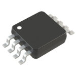 ZXMD63N03XTA
The activity of extra discounts on wholesale prices is in full swing…
Please fill in your contact information and we will send you the latest wholesale price list.





