 ChipApex | Global Electronic Components Supplier
SEARCH
Search Product
Search Post
— IC芯片 | 连接器 | 传感器 | 被动器件 —
Search productSearch post
— IC芯片 | 连接器 | 传感器 | 被动器件 —
Consult the customer manager about the wholesale price.
consultation hotline:86-132-6715-2157
email:[email protected]
Contact the product manager for consultation. One-stop consultation is available.
Do you want a lower wholesale price? Please send us your inquiry and we will reply immediately.
The ZXMP6A16DN8QTA is a dual P-channel enhancement mode MOSFET from Diodes Incorporated, housed in an SO-8 package. It features a drain-source voltage of -60V and continuous drain currents of -3.9A at VGS = -10V and -3.2A at VGS = -4.5V. The device exhibits low on-resistance, with maximum values of 85mΩ at -10V gate drive and 125mΩ at -4.5V gate drive. Key electrical parameters include a total gate charge of 12.1nC at -10V, input capacitance of 1021pF, and a reverse recovery time of 29.2ns for the body diode. It operates within a temperature range of -55°C to +150°C and meets AEC-Q101 automotive standards.
Verify that the ordering suffix QTA corresponds to the specified automotive qualification and tape & reel packaging format. Confirm compliance with RoHS directives and PPAP availability requirements before finalizing procurement specifications. Ensure the component matches the exact DS36687 Rev. 2 datasheet version to guarantee parameter consistency.
Select this component when a dual P-channel solution is required in an SO-8 footprint. Evaluate thermal derating curves for PCB layout constraints, as power dissipation depends heavily on copper coverage. Verify that the gate drive voltage supports the desired RDS(ON) threshold, noting the difference between -10V and -4.5V operation points.
This part belongs to the ZXMN6/ZXMP6 series of power MOSFETs from Diodes Incorporated. It serves as a dual-channel variant optimized for space-constrained designs requiring independent control of two P-channel paths. The 'Q' suffix indicates automotive-grade qualification, distinguishing it from standard commercial variants.
Direct substitutes must match the dual P-channel topology, -60V rating, and SO-8 package. Check equivalent RDS(ON) values at specific gate voltages (-10V/-4.5V). Verify pinout compatibility, particularly the shared source/drain configurations in the SO-8 outline. Cross-reference thermal resistance (RθJA) if operating near maximum junction temperatures.
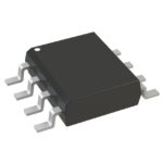 ZXMP6A16DN8QTA
The activity of extra discounts on wholesale prices is in full swing…
Please fill in your contact information and we will send you the latest wholesale price list.





