 ChipApex | Global Electronic Components Supplier

SEARCH
Search Product
Search Post
— IC芯片 | 连接器 | 传感器 | 被动器件 —
Search productSearch post
— IC芯片 | 连接器 | 传感器 | 被动器件 —
Consult the customer manager about the wholesale price.
consultation hotline:86-132-6715-2157
email:[email protected]
Contact the product manager for consultation. One-stop consultation is available.
Do you want a lower wholesale price? Please send us your inquiry and we will reply immediately.
The onsemi 2N5551YBU is a discontinued NPN general-purpose amplifier transistor housed in a TO-92-3 (Case 135AN) through-hole package. It features a collector-emitter voltage of 160 V, continuous collector current of 600 mA, and total device dissipation of 625 mW. The 'Y' suffix specifies a DC current gain (hFE) range of 180 to 240 at IC = 10 mA and VCE = 5.0 V. Electrical characteristics include a collector-base breakdown voltage of 180 V, emitter-base breakdown voltage of 6.0 V, and a current gain bandwidth product of 100 MHz.
Verify the discontinuation status directly with onsemi or authorized distributors before design finalization. Confirm that the TO-92-3 Case 135AN package dimensions match the target PCB footprint. Ensure the specific Y-bin gain requirements are compatible with the circuit design, as standard non-Y variants offer different gain ranges.
Select this component when a high-voltage NPN transistor with elevated DC current gain is required for through-hole assembly. The 160 V rating supports high-side switching or amplification tasks. Designers must account for the 625 mW power dissipation limit and derating requirements above 25°C ambient temperature to maintain reliability within the specified -55°C to +150°C junction temperature range.
The 2N5551 series comprises NPN silicon planar epitaxial transistors intended for general-purpose use. The 2N5551YBU represents a specific manufacturing lot configuration with defined gain characteristics. It belongs to the broader family of small-signal bipolar junction transistors produced by onsemi for discrete semiconductor applications.
Consult onsemi representatives for current available alternatives. Standard 2N5551BU devices share the same package and electrical ratings but lack the specific 180-240 hFE gain binning associated with the Y suffix.
The 'Y' suffix denotes a specific DC current gain (hFE) range of 180 to 240, tested at IC = 10 mA and VCE = 5.0 V.
No, the 2N5551YBU has been officially discontinued by onsemi as of January 2026.
The maximum collector-emitter voltage (VCEO) is rated at 160 V.
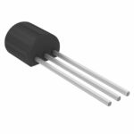 2N5551YBU

The activity of extra discounts on wholesale prices is in full swing…
Please fill in your contact information and we will send you the latest wholesale price list.





