ChipApex | Global Electronic Components Supplier
SEARCH
Search Product
Search Post
— IC芯片 | 连接器 | 传感器 | 被动器件 —
Search productSearch post
— IC芯片 | 连接器 | 传感器 | 被动器件 —
Consult the customer manager about the wholesale price.
consultation hotline:86-132-6715-2157
email:[email protected]
Contact the product manager for consultation. One-stop consultation is available.
Do you want a lower wholesale price? Please send us your inquiry and we will reply immediately.
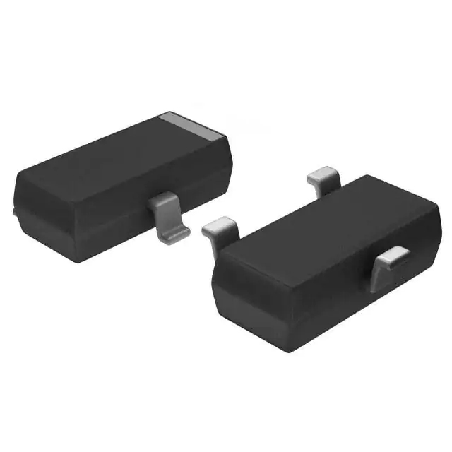
The 2N7002EY is an N-Channel Enhancement Mode MOSFET manufactured by ANBON SEMICONDUCTOR (INT'L) LIMITED. It utilizes Trench Power MV MOSFET technology and is housed in a SOT-23 package. The device features a drain-source voltage rating of 60 V, a continuous drain current of 0.3 A, and a maximum power dissipation of 0.3 W. Key electrical parameters include a gate-source breakdown voltage of ±20 V, a typical gate threshold voltage of 1.5 V, and a maximum on-resistance of 2.5 Ω at VGS=10V. Dynamic characteristics specify a total gate charge of 1.22 nC and an input capacitance of 21 pF.
Verify the manufacturer designation as ANBON SEMICONDUCTOR (INT'L) LIMITED against the specific datasheet AS-3150428 Revision B. Confirm that the component matches the SOT-23 package dimensions and the electrical ratings provided in the official documentation before integration into designs.
Select this component for applications requiring low input capacitance and fast switching speeds within a compact SOT-23 footprint. Ensure the design accommodates the 0.3 W power dissipation limit and the thermal resistance of 416 °C/W when mounted on standard FR-4 PCBs.
This part belongs to the family of N-Channel Enhancement Mode MOSFETs designed for general-purpose small-signal switching. The SOT-23 package provides a surface-mount solution suitable for space-constrained electronic circuits requiring reliable voltage-controlled operation.
Cross-reference with other 60V N-Channel MOSFETs in SOT-23 packages. Verify compatibility regarding RDS(on), Qg, and package pinout if substituting with components from different manufacturers.
The maximum pulsed drain current is 1.5 A.
The reverse recovery time is 16 ns under specified test conditions.
 2N7002EY
The activity of extra discounts on wholesale prices is in full swing…
Please fill in your contact information and we will send you the latest wholesale price list.